- 您現(xiàn)在的位置:買賣IC網(wǎng) > PDF目錄360488 > 74LV4053PWDH (NXP SEMICONDUCTORS) Triple 2-channel analog multiplexer/demultiplexer PDF資料下載
參數(shù)資料
| 型號: | 74LV4053PWDH |
| 廠商: | NXP SEMICONDUCTORS |
| 元件分類: | 多路復(fù)用及模擬開關(guān) |
| 英文描述: | Triple 2-channel analog multiplexer/demultiplexer |
| 中文描述: | TRIPLE 2-CHANNEL, SGL ENDED MULTIPLEXER, PDSO16 |
| 封裝: | PLASTIC, TSSOP-16 |
| 文件頁數(shù): | 8/16頁 |
| 文件大小: | 154K |
| 代理商: | 74LV4053PWDH |
Philips Semiconductors
Product specification
74LV4053
Triple 2-channel analog multiplexer/demultiplexer
1998 Jun 23
8
ADDITIONAL AC CHARACTERISTICS
Recommended conditions and typical values
GND = 0 V; t
r
= t
f
≤
2.5ns
SYMBOL
PARAMETER
TYP.
UNIT
V
CC
(V)
3.0
6.0
3.0
6.0
3.0
6.0
3.0
6.0
3.0
6.0
V
is(p–p)
(V)
2.75
5.50
2.75
5.50
Note 1
CONDITIONS
Sine-wave distortion
f = 1 kHz
Sine-wave distortion
f = 10 kHz
Switch “OFF” signal feed through
0.80
0.40
2.40
1.20
–50
–50
–60
–60
110
120
%
R
= 10 k ; C
= 50 pf
Figures 9 and 10
R
= 10 k ; C
= 50 pf
Figures 9 and 10
R
= 600 ; C
= 50 pf; f= 1 MHz
Figures 5 and 11
R
= 600 ; C
L
= 50 pf; f= 1 MHz
Figure 8
R
L
= 600 ; C
= 50 pf; f= 1 MHz
(S
n
or E, square wave between V
CC
and GND t
r
= t
f
= 6 ns) Figure 8
R
L
= 50 ; C
L
= 50 pF
Figures 6, 8 and 9
%
dB
Crosstalk between any two
switches/multiplexers
Crosstalk voltage between enable or
address input to any switch
(peak-to-peak value)
Minimum frequency response
(–3 dB)
Maximum switch capacitance
GENERAL NOTES:
V
is
is the input voltage at nY
or nZ terminal, whichever is assigned as an input.
V
is the output voltage at nY
n
or nZ terminal, whichever is assigned as an output.
NOTES:
1.
Adjust input voltage V
is
is 0 dBm level (0 dBm = 1 mW into 600
2.
Adjust input voltage V
is
is 0 dBm level at V
OS
for 1 MHz (0 dBm = 1 mW into 50
dB
Note 1
V
(p–p)
mV
f
max
180
200
5
MHz
3.0
6.0
Note 2
C
S
pf
SV01635
(dB)
f (kHz)
0
10
10
2
10
3
10
4
10
5
10
6
–50
–100
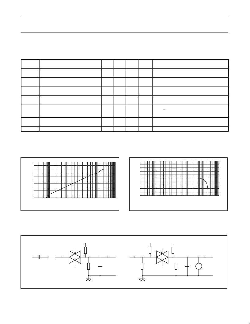
Figure 6. Typical switch “OFF” signal feed-through as a
function of frequency.
SV01636
(dB)
f (kHz)
5
10
10
2
10
3
10
4
10
5
10
6
0
–5
Figure 7. Typical frequency response.
NOTES TO FIGURES 6 AND 7:
Test conditions: V
CC
= 3.0 V; GND = 0 V; V
EE
= -3.0V; R
L
= 50 ; R
SOURCE
= 1k .
SV01663
GND
2R
L
V
CC
channel
ON
Vis
0.1 F
R
L
nY
n
/nZ
nZ/nY
n
C
L
GND
channel
OFF
(b)
(a)
V
os
dB
2R
L
nY
n
/nZ
2R
L
2R
L
V
CC
V
CC
nZ/nY
n
2R
L
C
L
R
L
Figure 8. Test circuit for measuring crosstalk between any two switches.
(a) channel ON condition; (b) channel OFF condition.
相關(guān)PDF資料 |
PDF描述 |
|---|---|
| 74LV4053 | Triple 2-channel analog multiplexer/demultiplexer(三2通道模擬多路復(fù)用器/多路分解器) |
| 74LV4060 | 14-stage binary ripple counter with oscillator(帶振蕩器的14級二進制紋波計數(shù)器) |
| 74LV4060PWDH | 14-stage binary ripple counter with oscillator |
| 74LV4066 | Quad bilateral switches(四雙向開關(guān)) |
| 74LV4094 | 8-stage shift-and-store bus register(8級移位--存儲總線寄存器) |
相關(guān)代理商/技術(shù)參數(shù) |
參數(shù)描述 |
|---|---|
| 74LV4053PW-Q100J | 制造商:NXP Semiconductors 功能描述:74LV4053PW-Q100/TSSOP16/REEL13 - Tape and Reel 制造商:NXP Semiconductors 功能描述:IC MUX/DEMUX TRIPLE 2X1 16TSSOP |
| 74LV4053PW-T | 功能描述:多路器開關(guān) IC TRIPLE 2-CHANNEL MUX/DMUX RoHS:否 制造商:Texas Instruments 通道數(shù)量:1 開關(guān)數(shù)量:4 開啟電阻(最大值):7 Ohms 開啟時間(最大值): 關(guān)閉時間(最大值): 傳播延遲時間:0.25 ns 工作電源電壓:2.3 V to 3.6 V 工作電源電流: 最大工作溫度:+ 85 C 安裝風(fēng)格:SMD/SMT 封裝 / 箱體:UQFN-16 |
| 74LV4060 | 制造商:PHILIPS 制造商全稱:NXP Semiconductors 功能描述:14-stage binary ripple counter with oscillator |
| 74LV4060D | 功能描述:計數(shù)器 IC 14ST BIN COUNTER/DIV RIPPLE-CARRY W/OSC RoHS:否 制造商:NXP Semiconductors 計數(shù)器類型:Binary Counters 邏輯系列:74LV 位數(shù):10 計數(shù)法: 計數(shù)順序: 工作電源電壓:1 V to 5.5 V 工作溫度范圍:- 40 C to + 125 C 封裝 / 箱體:SOT-109 封裝:Reel |
| 74LV4060D,112 | 功能描述:計數(shù)器 IC 14ST BIN COUNTER/DIV RoHS:否 制造商:NXP Semiconductors 計數(shù)器類型:Binary Counters 邏輯系列:74LV 位數(shù):10 計數(shù)法: 計數(shù)順序: 工作電源電壓:1 V to 5.5 V 工作溫度范圍:- 40 C to + 125 C 封裝 / 箱體:SOT-109 封裝:Reel |
發(fā)布緊急采購,3分鐘左右您將得到回復(fù)。