- 您現(xiàn)在的位置:買賣IC網 > PDF目錄360484 > 74LV107 (NXP Semiconductors N.V.) Dual JK flip-flop with reset; negative-edge trigger PDF資料下載
參數資料
| 型號: | 74LV107 |
| 廠商: | NXP Semiconductors N.V. |
| 英文描述: | Dual JK flip-flop with reset; negative-edge trigger |
| 中文描述: | 雙JK觸發(fā)器的復位觸發(fā)器,負邊沿觸發(fā) |
| 文件頁數: | 6/12頁 |
| 文件大?。?/td> | 121K |
| 代理商: | 74LV107 |
Philips Semiconductors
Product specification
74LV107
Dual JK flip-flop with reset; negative-edge trigger
1998 Apr 20
6
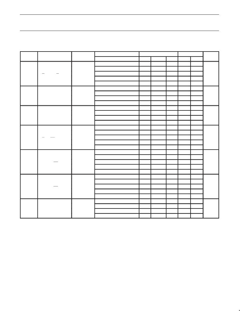
AC CHARACTERISTICS (Continued)
GND = 0V; t
r
= t
f
≤
2.5ns; C
L
= 50pF; R
L
= 1K
SYMBOL
PARAMETER
WAVEFORM
CONDITION
V
CC
(V)
1.2
2.0
2.7
3.0 to 3.6
4.5 to 5.5
2.0
2.7
3.0 to 3.6
4.5 to 5.5
2.0
2.7
3.0 to 3.6
4.5 to 5.5
1.2
2.0
2.7
3.0 to 3.6
4.5 to 5.5
1.2
2.0
2.7
3.0 to 3.6
4.5 to 5.5
1.2
2.0
2.7
3.0 to 3.6
4.5 to 5.5
2.0
2.7
3.0 to 3.6
4.5 to 5.5
–40 to +85
°
C
TYP
1
95
32
24
18
2
–40 to +125
°
C
MIN
UNIT
MIN
MAX
MAX
Propagation delay
nR to nQ, nQ
44
33
26
22
56
41
33
28
t
PHL
/t
PLH
Figures 1, 2
ns
34
25
20
15
34
25
20
15
14
10
8
2
41
30
24
18
41
30
24
t
W
Clock pulse width
HIGH or LOW
Figure 2
ns
14
10
8
2
t
W
Reset pulse width
LOW
Figure 2
ns
35
12
9
7
2
Removal time
nR to nCP
24
18
14
11
29
21
17
14
t
rem
Figure 2
ns
40
14
10
8
2
Set up time
Set-up time
nJ, nK to CP
26
19
15
12
31
23
18
15
t
su
Figure 1
ns
-10
–3
–2
–2
2
Hold time
nJ, nK to CP
5
5
5
5
14
19
24
30
5
5
5
5
12
16
20
24
t
h
Figure 1
ns
40
58
70
2
f
max
Maximum clock
pulse frequency
Figure 1
MHz
NOTES:
1. Unless otherwise stated, all typical values are measured at T
amb
= 25
°
C
2. Typical values are measured at V
CC
= 3.3 V.
相關PDF資料 |
PDF描述 |
|---|---|
| 74LV107D | CMOS/TTL Compatible |
| 74LV107DB | CMOS |
| 74LV107N | Dual JK flip-flop with reset; negative-edge trigger |
| 74LV107PW | CLP SINE |
| 74LV107PWDH | CLP SINE |
相關代理商/技術參數 |
參數描述 |
|---|---|
| 74LV107D | 制造商:PHILIPS 制造商全稱:NXP Semiconductors 功能描述:Dual JK flip-flop with reset; negative-edge trigger |
| 74LV107DB | 制造商:PHILIPS 制造商全稱:NXP Semiconductors 功能描述:Dual JK flip-flop with reset; negative-edge trigger |
| 74LV107DB-T | 制造商:未知廠家 制造商全稱:未知廠家 功能描述:J-K-Type Flip-Flop |
| 74LV107D-T | 制造商:未知廠家 制造商全稱:未知廠家 功能描述:J-K-Type Flip-Flop |
| 74LV107N | 制造商:PHILIPS 制造商全稱:NXP Semiconductors 功能描述:Dual JK flip-flop with reset; negative-edge trigger |
發(fā)布緊急采購,3分鐘左右您將得到回復。