- 您現(xiàn)在的位置:買賣IC網(wǎng) > PDF目錄375076 > 74LCX32374GX (FAIRCHILD SEMICONDUCTOR CORP) Low Voltage 32-Bit D-Type Flip-Flop with 5V Tolerant Inputs and Outputs Preliminary PDF資料下載
參數(shù)資料
| 型號(hào): | 74LCX32374GX |
| 廠商: | FAIRCHILD SEMICONDUCTOR CORP |
| 元件分類: | 通用總線功能 |
| 英文描述: | Low Voltage 32-Bit D-Type Flip-Flop with 5V Tolerant Inputs and Outputs Preliminary |
| 中文描述: | LVC/LCX/Z SERIES, QUAD 8-BIT DRIVER, TRUE OUTPUT, PBGA96 |
| 封裝: | 5.50 MM, PLASTIC, MO-205, FBGA-96 |
| 文件頁(yè)數(shù): | 2/8頁(yè) |
| 文件大小: | 189K |
| 代理商: | 74LCX32374GX |
Preliminary
www.fairchildsemi.com
2
7
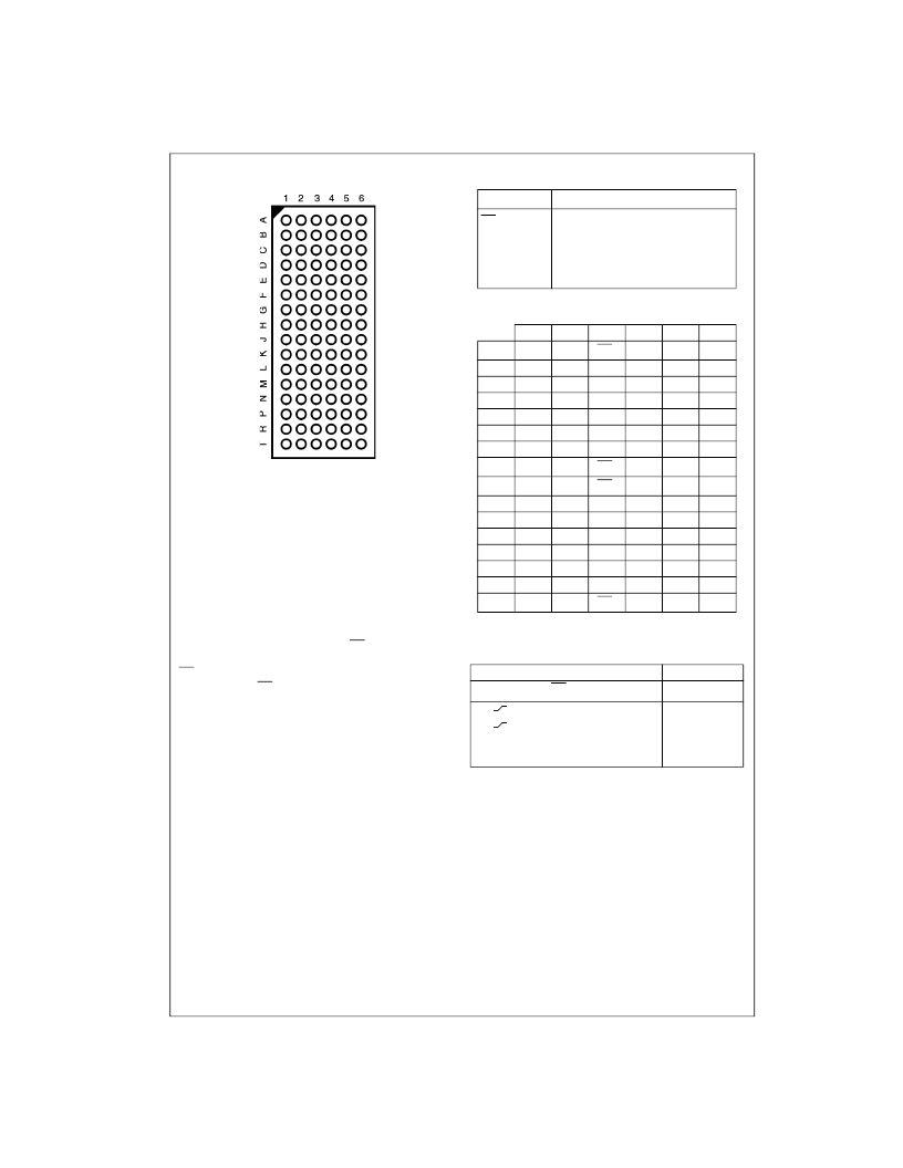
Connection Diagram
(Top Thru View)
Functional Description
The LCX32374 consists of thirty-two edge-triggered
flip-flops with individual D-type inputs and 3-STATE true
outputs. The device is byte controlled with each byte func-
tioning identically, but independent of the other. The control
pins can be shorted together to obtain full 32-bit operation.
Each byte has a buffered clock and buffered Output Enable
common to all flip-flops within that byte. The description
which follows applies to each byte. Each flip-flop will store
the state of their individual D inputs that meet the setup and
hold time requirements on the LOW-to-HIGH Clock (CP
n
)
transition. With the Output Enable (OE
n
) LOW, the con-
tents of the flip-flops are available at the outputs. When
OE
n
is HIGH, the outputs go to the high impedance state.
Operation of the OE
n
input does not affect the state of the
flip-flops.
Pin Descriptions
FBGA Pin Assignments
Truth Table
X
=
Immaterial
Z
=
High Impedance
O
0
=
Previous O
0
before HIGH-to-LOW of CP
Pin Names
Description
OE
n
CP
n
I
0
–
I
31
O
0
–
O
31
Output Enable Input (Active LOW)
Clock Pulse Input
Inputs
Outputs
1
2
3
4
5
6
A
B
C
D
E
F
G
O
1
O
3
O
5
O
7
O
9
O
11
O
13
O
14
O
17
O
19
O
21
O
23
O
25
O
27
O
29
O
30
O
0
O
2
O
4
O
6
O
8
O
10
O
12
O
15
O
16
O
18
O
20
O
22
O
24
O
26
O
28
O
31
OE
1
GND
V
CC
GND
GND
V
CC
GND
CP
1
GND
V
CC
GND
GND
V
CC
GND
I
0
I
2
I
4
I
6
I
8
I
10
I
12
I
15
I
16
I
18
I
20
I
22
I
24
I
26
I
28
I
31
I
1
I
3
I
5
I
7
I
9
I
11
I
13
I
14
I
17
I
19
I
21
I
23
I
25
I
27
I
29
I
30
H
OE
2
OE
3
GND
V
CC
GND
GND
V
CC
GND
CP
2
CP
3
GND
V
CC
GND
GND
V
CC
GND
J
K
L
M
N
P
R
T
OE
4
CP
4
Inputs
Outputs
CP
n
OE
n
L
L
L
H
I
n
H
L
X
X
O
n
H
L
O
0
Z
L
X
相關(guān)PDF資料 |
PDF描述 |
|---|---|
| 74LCX32374 | Low Voltage 32-Bit D-Type Flip-Flop with 5V Tolerant Inputs and Outputs Preliminary |
| 74LCX32646 | Low Voltage 32-Bit Transceiver/Register with 5V Tolerant Inputs and Outputs (Preliminary) |
| 74LCX32646GX | Low Voltage 32-Bit Transceiver/Register with 5V Tolerant Inputs and Outputs (Preliminary) |
| 74LCX32652 | Low Voltage Transceiver/Register with 5V Tolerant Inputs and Outputs (Preliminary) |
| 74LCX32652GX | Low Voltage Transceiver/Register with 5V Tolerant Inputs and Outputs (Preliminary) |
相關(guān)代理商/技術(shù)參數(shù) |
參數(shù)描述 |
|---|---|
| 74LCX32500 | 制造商:FAIRCHILD 制造商全稱:Fairchild Semiconductor 功能描述:Low Voltage 36-Bit Universal Bus Transceivers with 5V Tolerant Inputs and Outputs |
| 74LCX32500G | 功能描述:總線收發(fā)器 UB Transceiver LV 36Bit RoHS:否 制造商:Fairchild Semiconductor 邏輯類型:CMOS 邏輯系列:74VCX 每芯片的通道數(shù)量:16 輸入電平:CMOS 輸出電平:CMOS 輸出類型:3-State 高電平輸出電流:- 24 mA 低電平輸出電流:24 mA 傳播延遲時(shí)間:6.2 ns 電源電壓-最大:2.7 V, 3.6 V 電源電壓-最小:1.65 V, 2.3 V 最大工作溫度:+ 85 C 封裝 / 箱體:TSSOP-48 封裝:Reel |
| 74LCX32500GX | 功能描述:總線收發(fā)器 UB Transceiver LV 36Bit RoHS:否 制造商:Fairchild Semiconductor 邏輯類型:CMOS 邏輯系列:74VCX 每芯片的通道數(shù)量:16 輸入電平:CMOS 輸出電平:CMOS 輸出類型:3-State 高電平輸出電流:- 24 mA 低電平輸出電流:24 mA 傳播延遲時(shí)間:6.2 ns 電源電壓-最大:2.7 V, 3.6 V 電源電壓-最小:1.65 V, 2.3 V 最大工作溫度:+ 85 C 封裝 / 箱體:TSSOP-48 封裝:Reel |
| 74LCX32646 | 制造商:FAIRCHILD 制造商全稱:Fairchild Semiconductor 功能描述:Low Voltage 32-Bit Transceiver/Register with 5V Tolerant Inputs and Outputs (Preliminary) |
| 74LCX32646GX | 制造商:FAIRCHILD 制造商全稱:Fairchild Semiconductor 功能描述:Low Voltage 32-Bit Transceiver/Register with 5V Tolerant Inputs and Outputs (Preliminary) |
發(fā)布緊急采購(gòu),3分鐘左右您將得到回復(fù)。