- 您現(xiàn)在的位置:買賣IC網(wǎng) > PDF目錄360427 > 74F804 (NXP Semiconductors N.V.) Hex 2-input NAND drivers(六2輸入與非門驅(qū)動器) PDF資料下載
參數(shù)資料
| 型號: | 74F804 |
| 廠商: | NXP Semiconductors N.V. |
| 英文描述: | Hex 2-input NAND drivers(六2輸入與非門驅(qū)動器) |
| 中文描述: | 六角2輸入與非司機(jī)(六2輸入與非門驅(qū)動器) |
| 文件頁數(shù): | 4/8頁 |
| 文件大?。?/td> | 76K |
| 代理商: | 74F804 |
Philips Semiconductors
Product specification
74F804/1804
Hex 2-input NAND drivers
September 14, 1990
4
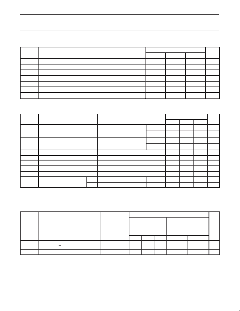
RECOMMENDED OPERATING CONDITIONS
SYMBOL
PARAMETER
LIMITS
T
A
=
–40 to
+85
°
C
V
UNIT
MIN
NOM
MAX
V
CC
V
IH
V
IL
I
Ik
I
OH
I
OL
Supply voltage
4.5
5.0
5.5
High–level input voltage
2.0
V
Low–level input voltage
0.8
V
Input clamp current
–18
mA
High–level output current
–48
mA
Low–level output current
48
mA
°
C
T
amb
Operating free air temperature range
0
+70
DC ELECTRICAL CHARACTERISTICS
(Over recommended operating free-air temperature range unless otherwise noted.)
SYMBOL
PARAMETER
TEST CONDITIONS
1
LIMITS
TYP
2
UNIT
MIN
MAX
V
OH
High-level output voltage
V
CC
= MIN, V
IL
= MAX
±
10%V
CC
±
5%V
CC
±
10%V
CC
±
5%V
CC
2.0
V
V
IH
= MIN, I
OH
= MAX
2.0
V
V
OL
Low-level output voltage
V
CC
= MIN, V
IL
= MAX
0.38
0.55
V
V
IH
= MIN, I
OL
= MAX
0.38
0.55
V
V
IK
I
I
I
IH
I
IL
I
O
I
CC
Input clamp voltage
Input current at maximum input voltage
V
CC
= MIN, I
I
= I
IK
V
CC
= MAX, V
I
= 7.0V
V
CC
= MAX, V
I
= 2.7V
V
CC
= MAX, V
I
= 0.5V
V
CC
= MAX
V
CC
= MAX
V
CC
= MAX
-0.73
-1.2
100
V
μ
A
μ
A
μ
A
High–level input current
20
Low–level input current
Output current
3
-20
-60
-160
mA
Supply current (total)
I
CCH
I
CCL
V
IN
= GND
V
IN
= 4.5V
2.0
3.0
mA
15
20
mA
NOTES:
1. For conditions shown as MIN or MAX, use the appropriate value specified under recommended operating conditions for the applicable type.
2. All typical values are at V
= 5V, T
= 25
°
C.
3. The output conditions have been chosen to produce a current that closely approximates one half of the true short–circuit output current, I
OS
.
AC ELECTRICAL CHARACTERISTICS
LIMITS
T
amb
= +25
°
C
V
CC
= +5.0V
C
L
= 50pF,
R
L
= 500
MIN
TYP
T
amb
= 0
°
C to +70
°
C
V
CC
= +5.0V
±
10%
C
L
= 50pF,
R
L
= 500
MIN
SYMBOL
PARAMETER
TEST
UNIT
CONDITION
MAX
MAX
t
PLH
t
PHL
t
sk(o)
NOTES:
1. [t
PN
actual – t
PM
actual] for any output compared to any other output where N and M are either LH or HL.
2. Skew times are valid only under same test conditions (temperature, V
CC
, loading, etc.,).
Propagation delay
Dna, Dnb to Qn
Output skew
1,2
Waveform 1
1.0
1.0
2.0
3.0
4.0
4.5
1.0
1.0
4.0
5.0
ns
Waveform 2
1.5
1.5
ns
相關(guān)PDF資料 |
PDF描述 |
|---|---|
| 74F1805 | Hex 2-input NOR drivers |
| 74F805 | Hex 2-input NOR drivers(六2輸入或非門驅(qū)動器) |
| 74F1808 | Hex 2-input AND drivers(六2輸入與門驅(qū)動器) |
| 74F808 | Hex 2-input AND drivers(六2輸入與門驅(qū)動器) |
| 74F181 | Arithmetic logic unit |
相關(guān)代理商/技術(shù)參數(shù) |
參數(shù)描述 |
|---|---|
| 74F805 | 制造商:PHILIPS 制造商全稱:NXP Semiconductors 功能描述:Hex 2-input NOR drivers |
| 74F807 | 制造商:PHILIPS 制造商全稱:NXP Semiconductors 功能描述:Octal shift/count registered transceiver with adder and parity 3.State |
| 74F808 | 制造商:PHILIPS 制造商全稱:NXP Semiconductors 功能描述:Hex 2-input AND drivers |
| 74F821 | 制造商:Texas Instruments 功能描述:74F821 |
| 74F821_00 | 制造商:FAIRCHILD 制造商全稱:Fairchild Semiconductor 功能描述:10-Bit D-Type Flip-Flop |
發(fā)布緊急采購,3分鐘左右您將得到回復(fù)。