- 您現(xiàn)在的位置:買賣IC網(wǎng) > PDF目錄375071 > 74F401SC (FAIRCHILD SEMICONDUCTOR CORP) CRC Generator/Checker PDF資料下載
參數(shù)資料
| 型號: | 74F401SC |
| 廠商: | FAIRCHILD SEMICONDUCTOR CORP |
| 元件分類: | 通用總線功能 |
| 英文描述: | CRC Generator/Checker |
| 中文描述: | F/FAST SERIES, 1-BIT CRC GENERATOR CKT, PDSO14 |
| 封裝: | 0.150 INCH, MS-120, SOIC-14 |
| 文件頁數(shù): | 2/7頁 |
| 文件大小: | 60K |
| 代理商: | 74F401SC |
www.fairchildsemi.com
2
7
Unit Loading/Fan Out
Functional Description
The 74F401 is a 16-bit programmable device which oper-
ates on serial data streams and provides a means of
detecting transmission errors. Cyclic encoding and decod-
ing schemes for error detection are based on polynomial
manipulation in modulo arithmetic. For encoding, the data
stream (message polynomial) is divided by a selected poly-
nomial. This division results in a remainder which is
appended to the message as check bits. For error check-
ing, the bit stream containing both data and check bits is
divided by the same selected polynomial. If there are no
detectable errors, this division results in a zero remainder.
Although it is possible to choose many generating polyno-
mials of a given degree, standards exist that specify a
small number of useful polynomials. The 74F401 imple-
ments the polynomials listed in Table 1 by applying the
appropriate logic levels to the select pins S
0,
S
1
and S
2
.
The 74F401 consists of a 16-bit register, a Read Only
Memory (ROM) and associated control circuitry as shown
in the block diagram. The polynomial control code pre-
sented at inputs S
0
, S
1
and S
2
is decoded by the ROM,
selecting the desired polynomial by establishing shift mode
operation on the register with Exclusive OR gates at appro-
priate inputs. To generate the check bits, the data stream is
entered via the Data inputs (D), using the HIGH-to-LOW
transition of the Clock input (CP). This data is gated with
the most significant output (Q) of the register, and controls
the Exclusive OR gates Figure 1. The Check Word Enable
(CWE) must be held HIGH while the data is being entered.
After the last data bit is entered, the CWE is brought LOW
and the check bits are shifted out of the register and
appended to the data bits using external gating Figure 2.
To check an incoming message for errors, both the data
and check bits are entered through the D input with the
CWE input held HIGH. The 74F401 is not in the data path,
but only monitors the message. The Error Output becomes
valid after the last check bit has been entered into the
74F401 by a HIGH-to-LOW transition of CP. If no detect-
able errors have occurred during the data transmission, the
resultant internal register bits are all LOW and the Error
Output (ER) is LOW. If a detectable error has occurred, ER
is HIGH.
A HIGH on the Master Reset input (MR) asynchronously
clears the register. A LOW on the Preset input (P) asyn-
chronously sets the entire register if the control code inputs
specify a 16-bit polynomial; in the case of 12- or 8-bit check
polynomials only the most significant 12 or 8 register bits
are set and the remaining bits are cleared.
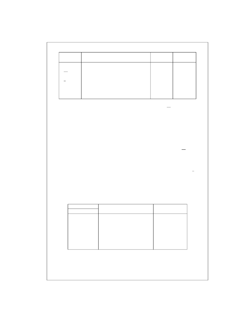
TABLE 1.
Pin Names
Description
U.L.
Input I
IH
/I
IL
Output I
OH
/I
OL
20
μ
A/
0.6 mA
20
μ
A/
0.6 mA
20
μ
A/
0.6 mA
20
μ
A/
0.6 mA
20
μ
A/
0.6 mA
20
μ
A/
0.6 mA
1 mA/20 mA
1 mA/20 mA
HIGH/LOW
1.0/1.0
1.0/1.0
1.0/1.0
S
0
–S
2
D
Polynomial Select Inputs
Data Input
Clock Input (Operates on HIGH-to-LOW Transition)
CP
CWE
Check Word Enable Input
Preset (Active LOW) Input
1.0/1.0
1.0/1.0
P
MR
Q
ER
Master Reset (Active HIGH) Input
Data Output
Error Output
1.0/1.0
50/33.3
50/33.3
Select Code
S
1
L
L
H
H
L
L
H
H
Polynomial
Remarks
S
2
L
L
L
L
H
H
H
H
S
0
L
H
L
H
L
H
L
H
X
16
+
X
15
+
X
2
+
1
X
16
+
X
14
+
X
+
1
X
16
+
X
15
+
X
13
+
X
7
+
X
4
+
X
2
+
X
1
+
1
X
12
+
X
11
+
X
3
+
X
2
+
X
+
1
X
8
+
X
7
+
X
5
+
X
4
+
X
+
1
X
8
+
1
X
16
+
X
12
+
X
5
+
1
X
16
+
X
11
+
X
4
+
1
CRC-16
CRC-16 REVERSE
CRC-12
LRC-8
CRC-CCITT
CRC-CCITT REVERSE
相關(guān)PDF資料 |
PDF描述 |
|---|---|
| 74F401SCX | CRC Generator/Checker |
| 74F403 | First-In First-Out (FIFO) Buffer Memory |
| 74F403A | First-In First-Out (FIFO) Buffer Memory |
| 74F403ASPC | First-In First-Out (FIFO) Buffer Memory |
| 74F433 | First-In First-Out (FIFO) Buffer Memory |
相關(guān)代理商/技術(shù)參數(shù) |
參數(shù)描述 |
|---|---|
| 74F401SCX | 功能描述:算數(shù)邏輯單元 - ALU CRC Gen/Checker RoHS:否 制造商:ON Semiconductor 高電平輸出電流: 低電平輸出電流: 傳播延遲時(shí)間: 電源電壓-最大:18 V 電源電壓-最小:3 V 封裝 / 箱體:SOIC-16 Wide 最大工作溫度:+ 125 C 封裝:Reel |
| 74F402 | 制造商:NSC 制造商全稱:National Semiconductor 功能描述:Serial Data Polynomial Generator/Checker |
| 74F402 WAF | 制造商:Fairchild Semiconductor Corporation 功能描述: |
| 74F402PC | 功能描述:算數(shù)邏輯單元 - ALU Ser Data Pol Gen/Che RoHS:否 制造商:ON Semiconductor 高電平輸出電流: 低電平輸出電流: 傳播延遲時(shí)間: 電源電壓-最大:18 V 電源電壓-最小:3 V 封裝 / 箱體:SOIC-16 Wide 最大工作溫度:+ 125 C 封裝:Reel |
| 74F403 | 制造商:FAIRCHILD 制造商全稱:Fairchild Semiconductor 功能描述:First-In First-Out (FIFO) Buffer Memory |
發(fā)布緊急采購,3分鐘左右您將得到回復(fù)。