- 您現在的位置:買賣IC網 > PDF目錄360435 > 74F3893 (NXP Semiconductors N.V.) Quad Futurebus backplane transceiver(四通道預置總線底板收發(fā)器) PDF資料下載
參數資料
| 型號: | 74F3893 |
| 廠商: | NXP Semiconductors N.V. |
| 英文描述: | Quad Futurebus backplane transceiver(四通道預置總線底板收發(fā)器) |
| 中文描述: | 四Futurebus背板收發(fā)器(四通道預置總線底板收發(fā)器) |
| 文件頁數: | 7/10頁 |
| 文件大?。?/td> | 72K |
| 代理商: | 74F3893 |
Philips Semiconductors
Product specification
74F3893
Quad Futurebus backplane transceiver
January 18, 1991
7
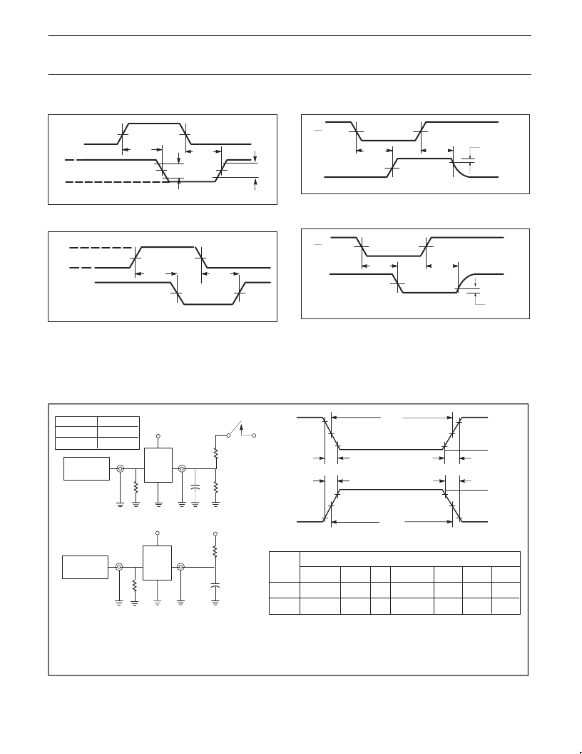
AC WAVEFORMS
V
M
V
M
V
M
V
M
I/On
DE, Dn
t
PHL
t
PLH
90%
10%
90%
10%
2V
t
TLH
t
THL
SF00577
1V
Waveform 1. Propagation delay for driver
V
M
V
M
V
M
V
M
Rn
I/On
t
PHL
t
PLH
2V
SF00578
1V
Waveform 2. Propagation delay for receiver
V
M
V
M
V
M
t
PHZ
t
PZH
V
OH
-0.3V
0V
RE
Rn
SF00579
Waveform 3. 3–state output enable time to high level
and output disable time from high level
V
M
V
M
V
M
t
PLZ
t
PZL
V
OL
+0.3V
SF00580
RE
Rn
Waveform 4. 3-state output enable time to low level
and output disable time from low level
Notes to AC waveforms
1. For all waveforms, V
M
= 1.5V.
2. The shaded areas indicate when the input is permitted to change for predictable output performance.
TEST CIRCUITS AND WAVEFORMS
t
w
90%
V
M
10%
90%
V
M
10%
90%
V
M
10%
90%
V
M
10%
NEGATIVE
PULSE
POSITIVE
PULSE
t
w
AMP (V)
Low V
Low V
t
THL (
t
f
)
INPUT PULSE REQUIREMENTS
rep. rate
t
w
t
TLH
t
THL
2.5ns
1MHz
500ns 2.5ns
Input pulse definition
V
CC
family
D port
D.U.T.
PULSE
GENERATOR
R
L
C
L
R
T
V
IN
V
OUT
Test circuit for 3–state outputs on D port
DEFINITIONS:
R
L
=
C
L
=
R
U
=
C
D
=
R
T
=
Load resistor; see AC electrical characteristics for value.
Load capacitance includes jig and probe capacitance; see AC electrical characteristics for value.
Pull up resistor; see AC Electrical Characteristics for value.
Load capacitance includes jig and probe capacitance; see AC electrical characteristics for value.
Termination resistance should be equal to Z
OUT
of pulse generators.
t
THL (
t
f
)
t
TLH (
t
r
)
t
TLH (
t
r
)
AMP (V)
amplitude
3.0V
1.5V
V
M
R
L
7.0V
V
CC
D.U.T.
PULSE
GENERATOR
C
D
R
T
V
IN
V
OUT
Test circuit for outputs on I/O port
R
T
7.0V
1MHz
500ns
I/O port
2.0V
1.5V
4.0ns
4.0ns
Low V
0.0V
1.0V
SWITCH POSITION
TEST
t
PLZ
, t
PZL
SWITCH
closed
open
All other
SF00581
相關PDF資料 |
PDF描述 |
|---|---|
| 74F38DC | Quad 2-input NAND Gate |
| 54F38LMQB | Quad 2-input NAND Gate |
| 74F38SCX | Quad 2-input NAND Gate |
| 74F38SJX | Quad 2-input NAND Gate |
| 74F38SC | Quad Two-Input NAND Buffer (Open Collector) |
相關代理商/技術參數 |
參數描述 |
|---|---|
| 74F38D | 制造商:NXP Semiconductors 功能描述:2INPUT NAND BUFFR(OPEN COLL.) |
| 74F38DC | 制造商:未知廠家 制造商全稱:未知廠家 功能描述:Quad 2-input NAND Gate |
| 74F38N | 制造商:NXP Semiconductors 功能描述:2INPUT NAND BUFFR(OPEN COLL.) |
| 74F38PC | 功能描述:邏輯門 Qd 2-Input NAND Buf RoHS:否 制造商:Texas Instruments 產品:OR 邏輯系列:LVC 柵極數量:2 線路數量(輸入/輸出):2 / 1 高電平輸出電流:- 16 mA 低電平輸出電流:16 mA 傳播延遲時間:3.8 ns 電源電壓-最大:5.5 V 電源電壓-最小:1.65 V 最大工作溫度:+ 125 C 安裝風格:SMD/SMT 封裝 / 箱體:DCU-8 封裝:Reel |
| 74F38PC_Q | 功能描述:邏輯門 Qd 2-Input NAND Buf RoHS:否 制造商:Texas Instruments 產品:OR 邏輯系列:LVC 柵極數量:2 線路數量(輸入/輸出):2 / 1 高電平輸出電流:- 16 mA 低電平輸出電流:16 mA 傳播延遲時間:3.8 ns 電源電壓-最大:5.5 V 電源電壓-最小:1.65 V 最大工作溫度:+ 125 C 安裝風格:SMD/SMT 封裝 / 箱體:DCU-8 封裝:Reel |
發(fā)布緊急采購,3分鐘左右您將得到回復。