- 您現(xiàn)在的位置:買(mǎi)賣(mài)IC網(wǎng) > PDF目錄360427 > 74F175AD (NXP SEMICONDUCTORS) Quad D flip-flop PDF資料下載
參數(shù)資料
| 型號(hào): | 74F175AD |
| 廠商: | NXP SEMICONDUCTORS |
| 元件分類(lèi): | 通用總線功能 |
| 英文描述: | Quad D flip-flop |
| 中文描述: | F/FAST SERIES, POSITIVE EDGE TRIGGERED D FLIP-FLOP, COMPLEMENTARY OUTPUT, PDSO16 |
| 封裝: | PLASTIC, SOT-109, SO-16 |
| 文件頁(yè)數(shù): | 4/10頁(yè) |
| 文件大小: | 82K |
| 代理商: | 74F175AD |
Philips Semiconductors
Product specification
74F175A
Quad D flip-flop
1996 Mar 12
4
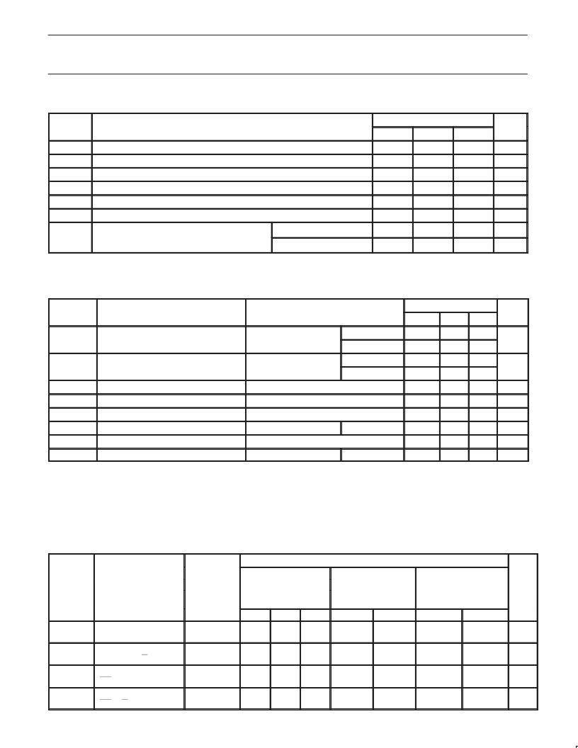
RECOMMENDED OPERATING CONDITIONS
SYMBOL
PARAMETER
LIMITS
UNIT
MIN
NOM
MAX
V
CC
V
IH
V
IL
I
IK
I
OH
I
OL
Supply voltage
4.5
5.0
5.5
V
High-level input voltage
2.0
V
Low-level input voltage
0.8
V
Input clamp current
–18
mA
High-level output current
–1
mA
Low-level output current
20
mA
°
C
°
C
T
amb
Operating free air temperature range
Commercial range
0
+70
Industrial range
–40
+85
DC ELECTRICAL CHARACTERISTICS
(Over recommended operating free-air temperature range unless otherwise noted.)
SYMBOL
PARAMETER
TEST
LIMITS
UNIT
CONDITIONS
1
MIN
TYP
2
MAX
V
OH
High-level output voltage
High-level out ut voltage
V
= MIN, V
= MAX,
CC
V
IH
= MIN, I
OH
= MAX
10%V
CC
5%V
CC
10%V
CC
5%V
CC
2.5
V
IL
2.7
3.4
V
OL
Low-level output voltage
V
= MIN, V
= MAX,
CC
V
IH
= MIN, I
OL
= MAX
0.30
0.5
V
IL
0.30
0.5
V
IK
I
I
I
IH
I
IL
I
OS
I
CC
Input clamp voltage
V
CC
= MIN, I
I
= I
IK
V
CC
= 0.0V, V
I
= 7.0V
V
CC
= MAX, V
I
= 2.7V
V
CC
= MAX, V
I
= 0.5V
V
CC
= MAX
V
CC
= MAX
–0.73
–1.2
V
Input current at maximum input voltage
100
μ
A
μ
A
High-level input current
20
Low-level input current
74F175A
–20
μ
A
Short-circuit output current
3
–60
–150
mA
Supply current (total)
74F175A
22
31
mA
Notes to DC electrical characteristics
1. For conditions shown as MIN or MAX, use the appropriate value specified under recommended operating conditions for the applicable type.
2. All typical values are at V
CC
= 5V, T
amb
= 25
°
C.
3. Not more than one output should be shorted at a time. For testing I
OS
, the use of high-speed test apparatus and/or sample-and-hold
techniques are preferable in order to minimize internal heating and more accurately reflect operational values. Otherwise, prolonged shorting
of a high output may raise the chip temperature well above normal and thereby cause invalid readings in other parameter tests. In any
sequence of parameter tests, I
OS
tests should be performed last.
AC ELECTRICAL CHARACTERISTICS FOR 74F175A
LIMITS
T
amb
= 25
°
C
V
CC
= +5V
C
L
= 50pF,
R
L
= 500
TYP
T
amb
= 0
°
C to +70
°
C
V
CC
= +5.0V
±
10%
C
L
= 50pF,
R
L
= 500
MIN
T
amb
=
V
CC
= +5.0V
±
10%
C
L
= 50pF,
R
L
= 500
MIN
40
°
C to +85
°
C
SYMBOL
PARAMETER
TEST
UNIT
CONDITION
MIN
MAX
MAX
MAX
f
max
Maximum clock
frequency
Waveform 1
140
160
125
110
MHz
t
PLH
t
PHL
Propagation delay
CP to Qn or Qn
Waveform 1
3.0
4.5
4.0
6.0
6.5
8.5
2.5
4.0
7.5
9.0
2.5
4.0
8.0
10.0
ns
t
PLH
t
PHL
Propagation delay
MR to Qn
Waveform 3
4.5
6.5
9.0
4.5
10.0
4.5
11.0
ns
t
PHL
t
PHL
Propagation delay
MR to Qn
Waveform 3
4.5
6.0
8.0
4.0
9.0
4.0
10.0
ns
相關(guān)PDF資料 |
PDF描述 |
|---|---|
| 74F175AN | Quad D flip-flop |
| 74F1763 | Intelligent DRAM controller IDC |
| 74F1779 | 8-bit bidirectional binary counter -State |
| 74F1804 | Hex 2-input NAND drivers |
| 74F804 | Hex 2-input NAND drivers(六2輸入與非門(mén)驅(qū)動(dòng)器) |
相關(guān)代理商/技術(shù)參數(shù) |
參數(shù)描述 |
|---|---|
| 74F175AN | 制造商:NXP Semiconductors 功能描述: 制造商:NXP Semiconductors 功能描述:Flip Flop, Quad, D Type, 16 Pin, Plastic, DIP |
| 74F175D | 制造商:Motorola 功能描述:74F175 MOT S1I2A 制造商:NXP Semiconductors 功能描述: 制造商:North American Philips Discrete Products Div 功能描述:74F175D 制造商:NXP Semiconductors 功能描述:74F175D |
| 74F175DC | 制造商:未知廠家 制造商全稱(chēng):未知廠家 功能描述:Quad D-Type Flip-Flop |
| 74F175LC | 制造商:Rochester Electronics LLC 功能描述:- Bulk |
| 74F175N | 制造商:North American Philips Discrete Products Div 功能描述:Flip Flop, Quad, D Type, 16 Pin, Plastic, DIP 制造商:NXP Semiconductors 功能描述:Flip Flop, Quad, D Type, 16 Pin, Plastic, DIP |
發(fā)布緊急采購(gòu),3分鐘左右您將得到回復(fù)。