- 您現(xiàn)在的位置:買賣IC網(wǎng) > PDF目錄375066 > 74ACTQ16240 (Fairchild Semiconductor Corporation) GTLP-to-LVTTL 1-to-6 Fanout Driver 24-SOIC -40 to 85 PDF資料下載
參數(shù)資料
| 型號: | 74ACTQ16240 |
| 廠商: | Fairchild Semiconductor Corporation |
| 英文描述: | GTLP-to-LVTTL 1-to-6 Fanout Driver 24-SOIC -40 to 85 |
| 中文描述: | 16位反向緩沖器/線路驅(qū)動器3態(tài)輸出 |
| 文件頁數(shù): | 3/7頁 |
| 文件大小: | 71K |
| 代理商: | 74ACTQ16240 |
3
www.fairchildsemi.com
7
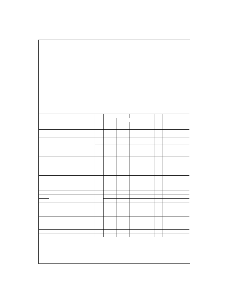
Absolute Maximum Ratings
(Note 1)
Recommended Operating
Conditions
Note 1:
Absolute maximum ratings are those values beyond which damage
to the device may occur. The databook specifications should be met, with-
out exception to ensure that the system design is reliable over its power
supply, temperature, and output/input loading variables. Fairchild does not
recommend operation of FACT
circuits outside databook specifications.
DC Electrical Characteristics
Note 2:
All outputs loaded; thresholds associated with output under test.
Note 3:
Maximum test duration 2.0 ms; one output loaded at a time.
Note 4:
Worst case package.
Note 5:
Maximum number of outputs that can switch simultaneously is n. (n
1) outputs are switched LOW and one output held LOW.
Note 6:
Maximum number of outputs that can switch simultaneously is n. (n
1) outputs are switched HIGH and one output held HIGH.
Note 7:
Maximum number of data inputs (n) switching. (n
1) input switching 0V to 3V. Input under test switching 3V to threshold (V
ILD
).
Supply Voltage (V
CC
)
DC Input Diode Current (I
IK
)
V
I
=
0.5V
V
I
=
V
CC
+
0.5V
DC Output Diode Current (I
OK
)
V
O
=
0.5V
V
O
=
V
CC
+
0.5V
DC Output Voltage (V
O
)
DC Output Source/Sink Current (I
O
)
DC V
CC
or Ground Current
per Output Pin
Junction Temperature
Storage Temperature
0.5V to
+
7.0V
20 mA
+
20 mA
20 mA
+
20 mA
0.5V to V
CC
+
0.5V
±
50 mA
±
50 mA
+
140
°
C
65
°
C to
+
150
°
C
Supply Voltage (V
CC
)
Input Voltage (V
I
)
Output Voltage (V
O
)
Operating Temperature (T
A
)
Minimum Input Edge Rate (
V/
t)
V
IN
from 0.8V to 2.0V
V
CC
@ 4.5V, 5.5V
4.5V to 5.5V
0V to V
CC
0V to V
CC
40
°
C to
+
85
°
C
125 mV/ns
Symbol
Parameter
V
CC
(V)
4.5
5.5
T
A
=
+
25
°
C
Typ
1.5
1.5
T
A
=
40
°
C to
+
85
°
C
Guaranteed Limits
Units
Conditions
V
IH
Minimum High
Input Voltage
2.0
2.0
2.0
2.0
V
V
OUT
=
0.1V
or V
CC
0.1V
V
OUT
=
0.1V
or V
CC
0.1V
I
OUT
=
50
μ
A
V
IL
Maximum Low
Input Voltage
Minimum High
4.5
5.5
4.5
1.5
1.5
4.49
0.8
0.8
4.4
0.8
0.8
4.4
V
V
OH
V
Output Voltage
5.5
5.49
5.4
5.4
V
IN
=
V
IL
or V
IH
I
OH
=
24 mA
I
OH
=
24 mA (Note 2)
I
OUT
=
50
μ
A
4.5
3.86
3.76
V
5.5
4.5
5.5
4.86
0.1
0.1
4.76
0.1
0.1
V
OL
Maximum Low
Output Voltage
0.001
0.001
V
V
IN
=
V
IL
or V
IH
I
OL
=
24 mA
I
OL
=
24 mA (Note 2)
V
I
=
V
IL
, V
IH
V
O
=
V
CC
, GND
V
I
=
V
CC
, GND
V
I
=
V
CC
2.1V
V
IN
=
V
CC
or GND
V
OLD
=
1.65V Max
V
OHD
=
3.85V Min
Figure 1Figure 2
(Note 5)(Note 6)
4.5
5.5
0.36
0.36
±
0.5
0.44
0.44
±
5.0
V
I
OZ
Maximum 3-STATE
Leakage Current
Maximum Input Leakage Current
5.5
μ
A
I
IN
I
CCT
I
CC
I
OLD
I
OHD
V
OLP
5.5
±
0.1
±
1.0
1.5
80.0
75
75
μ
A
mA
μ
A
mA
Maximum I
CC
/Input
Max Quiescent Supply Current
Minimum Dynamic
5.5
5.5
5.5
0.6
8.0
Output Current (Note 3)
Quiet Output
Maximum Dynamic V
OL
Quiet Output Minimum Dynamic V
OL
mA
V
5.0
0.5
0.8
V
OLV
5.0
0.5
1.0
V
Figure 1Figure 2
(Note 5)(Note 6)
Figure 1Figure 2
(Note 4)(Note 6)
Figure 1Figure 2
(Note 4)(Note 6)
V
OHP
Maximum Overshoot
5.0
V
OH
+
1.0
V
OH
+
1.5
V
V
OHV
Minimum V
CC
Droop
5.0
V
OH
1.0
V
OH
1.8
V
V
IHD
V
ILD
Minimum High Dynamic Input Voltage Level
Maximum Low Dynamic Input Voltage Level
5.0
5.0
1.7
1.2
2.0
0.8
V
V
(Note 4)(Note 7)
(Note 4)(Note 7)
相關(guān)PDF資料 |
PDF描述 |
|---|---|
| 74ACTQ16240MTD | GTLP-to-LVTTL 1-to-6 Fanout Driver 24-SOIC -40 to 85 |
| 74ACTQ16240MTDX | Quad 4-Bit Buffer/Driver |
| 74ACTQ16240SSC | 20 Characters x 4 Lines, 5x7 Dot Matrix Character and Cursor |
| 74ACTQ16244MTDX | Quad 4-Bit Buffer/Driver |
| 74ACTQ16244 | 16-Bit Buffer/Line Driver with 3-STATE Outputs |
相關(guān)代理商/技術(shù)參數(shù) |
參數(shù)描述 |
|---|---|
| 74ACTQ16240_YDC3026B WAF | 制造商:Fairchild Semiconductor Corporation 功能描述: |
| 74ACTQ16240_YDC3116B WAF | 制造商:Fairchild Semiconductor Corporation 功能描述: |
| 74ACTQ16240MTD | 功能描述:緩沖器和線路驅(qū)動器 16-Bit Buf/Line Drv RoHS:否 制造商:Micrel 輸入線路數(shù)量:1 輸出線路數(shù)量:2 極性:Non-Inverting 電源電壓-最大:+/- 5.5 V 電源電壓-最小:+/- 2.37 V 最大工作溫度:+ 85 C 安裝風(fēng)格:SMD/SMT 封裝 / 箱體:MSOP-8 封裝:Reel |
| 74ACTQ16240MTD_Q | 功能描述:緩沖器和線路驅(qū)動器 16-Bit Buf/Line Drv RoHS:否 制造商:Micrel 輸入線路數(shù)量:1 輸出線路數(shù)量:2 極性:Non-Inverting 電源電壓-最大:+/- 5.5 V 電源電壓-最小:+/- 2.37 V 最大工作溫度:+ 85 C 安裝風(fēng)格:SMD/SMT 封裝 / 箱體:MSOP-8 封裝:Reel |
| 74ACTQ16240MTDX | 功能描述:緩沖器和線路驅(qū)動器 16-Bit Buf/Line Drv RoHS:否 制造商:Micrel 輸入線路數(shù)量:1 輸出線路數(shù)量:2 極性:Non-Inverting 電源電壓-最大:+/- 5.5 V 電源電壓-最小:+/- 2.37 V 最大工作溫度:+ 85 C 安裝風(fēng)格:SMD/SMT 封裝 / 箱體:MSOP-8 封裝:Reel |
發(fā)布緊急采購,3分鐘左右您將得到回復(fù)。