- 您現(xiàn)在的位置:買賣IC網(wǎng) > PDF目錄382820 > 74ABT16500CSSCX (FAIRCHILD SEMICONDUCTOR CORP) 18-Bit Bus Transceiver PDF資料下載
參數(shù)資料
| 型號: | 74ABT16500CSSCX |
| 廠商: | FAIRCHILD SEMICONDUCTOR CORP |
| 元件分類: | 通用總線功能 |
| 英文描述: | 18-Bit Bus Transceiver |
| 中文描述: | ABT SERIES, 18-BIT REGISTERED TRANSCEIVER, TRUE OUTPUT, PDSO56 |
| 封裝: | 0.300 INCH, MO-118, SSOP-56 |
| 文件頁數(shù): | 1/9頁 |
| 文件大?。?/td> | 74K |
| 代理商: | 74ABT16500CSSCX |
April 1993
Revised January 1999
7
1999 Fairchild Semiconductor Corporation
DS011581.prf
www.fairchildsemi.com
74ABT16500
18-Bit Universal Bus Transceivers with 3-STATE Outputs
General Description
The ABT16500 18-bit universal bus transceiver combines
D-type latches and D-type flip-flops to allow data flow in
transparent, latched, and clocked modes.
Data flow in each direction is controlled by output-enable
(OEAB and OEBA), latch-enable (LEAB and LEBA), and
clock (CLKAB and CLKBA) inputs. For A-to-B data flow, the
device operates in the transparent mode when LEAB is
HIGH. When LEAB is LOW, the A data is latched if CLKAB
is held at a HIGH or LOW logic level. If LEAB is LOW, the A
bus data is stored in the latch/flip-flop on the HIGH-to-LOW
transition of CLKAB. Output-enable OEAB is active-high.
When OEAB is HIGH, the outputs are active. When OEAB
is LOW, the outputs are in the high-impedance state.
Data flow for B to A is similar to that of A to B but uses
OEBA, LEBA, and CLKBA. The output enables are com-
plementary (OEAB is active HIGH and OEBA is active
LOW).
To ensure the high-impedance state during power up or
power down, OE should be tied to GND through a pulldown
resistor; the minimum value of the resistor is determined by
the current-sourcing capability of the driver.
Features
I
Combines D-Type latches and D-Type flip-flops for
operation in transparent, latched, or clocked mode
I
Flow-through architecture optimizes PCB layout
I
Guaranteed latch-up protection
I
High impedance glitch free bus loading during entire
power up and power down cycle
I
Non-destructive hot insertion capability
Ordering Code:
Devices also available in Tape and Reel. Specify by appending the letter suffix “X” to the ordering code.
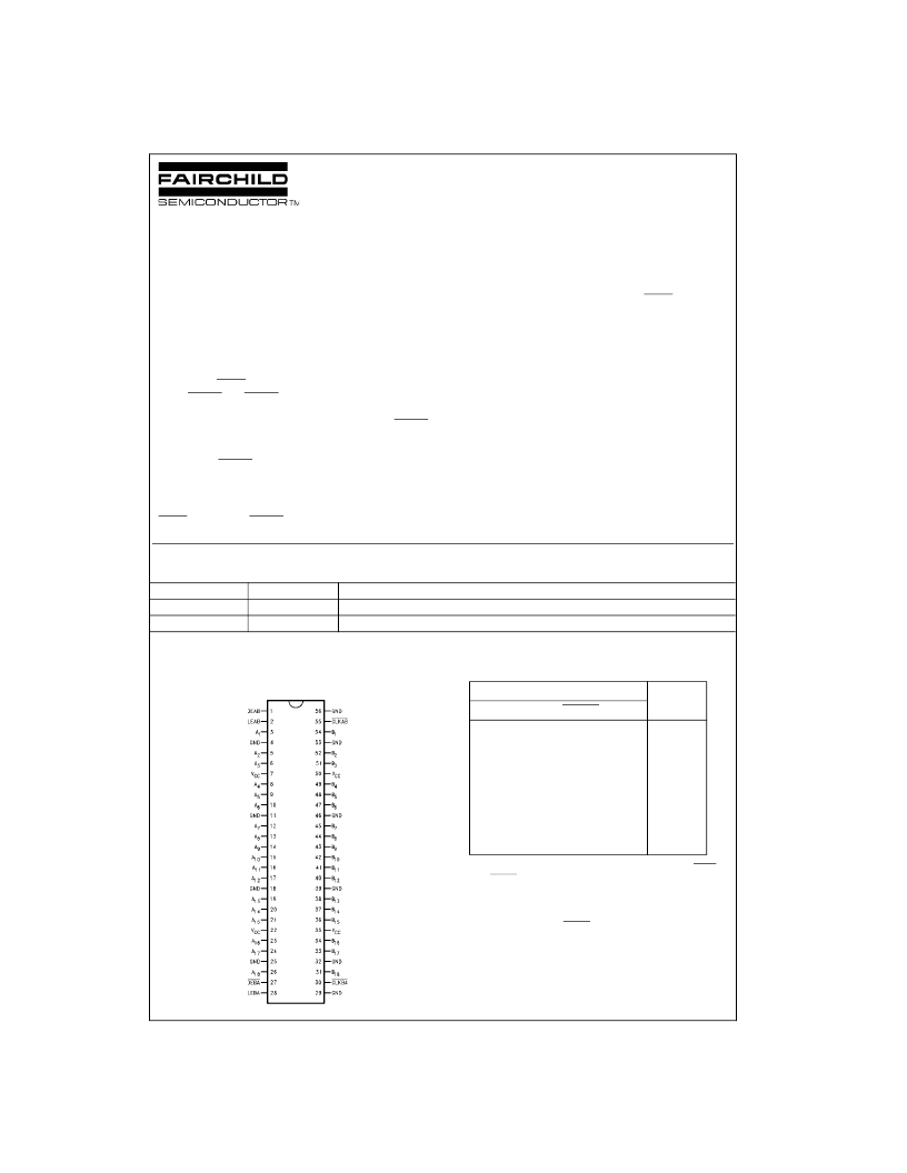
Connection Diagram
Pin Assignment for SSOP
Function Table
(Note 1)
Note 1:
A-to-B data flow is shown: B-to-A flow is similar but uses OEBA,
LEBA, and CLKBA.
Note 2:
Output level before the indicated steady-state input conditions
were established.
Note 3:
Output level before the indicated steady-state input conditions
were established, provided that CLKAB was LOW before LEAB went LOW.
Order Number
74ABT16500CSSC
74ABT16500CMTD
Package Number
MS56A
MTD56
Package Description
56-Lead Shrink Small Outline Package (SSOP), JEDEC MO-118, 0.300” Wide
56-Lead Thin Shrink Small Outline Package (TSSOP), JEDEC MO-153, 6.1mm Wide
Inputs
Output
OEAB
LEAB
CLKAB
A
B
L
X
X
X
Z
H
H
X
L
L
H
H
X
H
H
H
L
↓
L
L
H
L
↓
H
H
H
L
H
X
B
0
(Note 2)
B
0
(Note 3)
H
L
L
X
相關PDF資料 |
PDF描述 |
|---|---|
| 74AC08B | QUAD 2-INPUT AND GATE |
| 74AC08M | QUAD 2-INPUT AND GATE |
| 74AC399PC | Quad 2-Port Register |
| 74ACT399PC | Quad 2-Port Register |
| 74AC399SC | Quad 2-Port Register |
相關代理商/技術參數(shù) |
參數(shù)描述 |
|---|---|
| 74ABT16501 | 制造商:FAIRCHILD 制造商全稱:Fairchild Semiconductor 功能描述:18-Bit Universal Bus Transceivers with 3-STATE Outputs |
| 74ABT16501_ZAF3026B WAF | 制造商:Fairchild Semiconductor Corporation 功能描述: |
| 74ABT16501_ZAF3116B WAF | 制造商:Fairchild Semiconductor Corporation 功能描述: |
| 74ABT16501A | 制造商:PHILIPS 制造商全稱:NXP Semiconductors 功能描述:18-bit universal bus transceiver 3-State |
| 74ABT16501ADGG | 制造商:PHILIPS 制造商全稱:NXP Semiconductors 功能描述:18-bit universal bus transceiver 3-State |
發(fā)布緊急采購,3分鐘左右您將得到回復。