- 您現(xiàn)在的位置:買賣IC網(wǎng) > PDF目錄382819 > 7473 (Fairchild Semiconductor Corporation) Dual Master-Slave J-K Flip-Flops with Clear and Complementary Outputs PDF資料下載
參數(shù)資料
| 型號: | 7473 |
| 廠商: | Fairchild Semiconductor Corporation |
| 英文描述: | Dual Master-Slave J-K Flip-Flops with Clear and Complementary Outputs |
| 中文描述: | 雙主從JK觸發(fā)器明確和互補輸出 |
| 文件頁數(shù): | 2/3頁 |
| 文件大小: | 39K |
| 代理商: | 7473 |
www.fairchildsemi.com
2
D
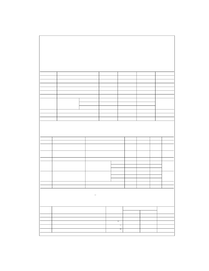
Absolute Maximum Ratings
(Note 1)
Note 1:
The “Absolute Maximum Ratings” are those values beyond which
the safety of the device cannot be guaranteed. The device should not be
operated at these limits. The parametric values defined in the Electrical
Characteristics tables are not guaranteed at the absolute maximum ratings.
The “Recommended Operating Conditions” table will define the conditions
for actual device operation.
Recommended Operating Conditions
Note 2:
The symbol (
↑
,
↓
) indicates the edge of the clock pulse is used for reference: (
↑
) for rising edge, (
↓
) for falling edge.
Note 3:
T
A
=
25
°
C and V
CC
=
5V.
Electrical Characteristics
over recommended operating free air temperature range (unless otherwise noted)
Symbol
Parameter
V
I
Input Clamp Voltage
V
OH
HIGH Level
Output Voltage
Note 4:
All typicals are at V
CC
=
5V, T
A
=
25
°
C.
Note 5:
Not more than one output should be shorted at a time.
Note 6:
With all outputs OPEN, I
CC
is measured with the Q and Q outputs HIGH in turn. At the time of measurement the clock input grounded.
Switching Characteristics
at V
CC
=
5V and T
A
=
25
°
C
Supply Voltage
Input Voltage
Operating Free Air Temperature Range
Storage Temperature Range
7V
5.5V
0
°
C to
+
70
°
C
65
°
C to
+
150
°
C
Symbol
V
CC
V
IH
V
IL
I
OH
I
OL
f
CLK
t
W
Parameter
Min
4.75
2
Nom
5
Max
5.25
Units
V
V
V
mA
mA
MHz
Supply Voltage
HIGH Level Input Voltage
LOW Level Input Voltage
HIGH Level Output Current
LOW Level Output Current
Clock Frequency (Note 3)
Pulse Width
(Note 3)
0.8
0.4
16
15
0
Clock HIGH
Clock LOW
Clear LOW
20
47
25
0
↑
0
↓
0
ns
t
SU
t
H
T
A
Input Setup Time (Note 2)(Note 3)
Input Hold Time (Note 2)(Note 3)
Free Air Operating Temperature
ns
ns
°
C
70
Conditions
Min
Typ (Note 4)
Max
1.5
Units
V
V
CC
=
Min, I
I
=
12 mA
V
CC
=
Min, I
OH
=
Max
V
IL
=
Max, V
IH
=
Min
V
CC
=
Min, I
OL
=
Max
V
IH
=
Min, V
IL
=
Max
2.4
3.4
V
V
OL
LOW Level
Output Voltage
Input Current @ Max Input Voltage V
CC
=
Max, V
I
=
5.5V
HIGH Level
Input Current
0.2
0.4
V
I
I
I
IH
1
mA
V
CC
=
Max
V
I
=
2.4V
J, K
Clock
Clear
40
80
80
1.6
3.2
3.2
55
34
μ
A
I
IL
LOW Level Input
Current
V
CC
=
Max
V
I
=
0.4V
J, K
Clock
Clear
mA
I
OS
I
CC
Short Circuit Output Current
Supply Current
V
CC
=
Max (Note 5)
V
CC
=
Max, (Note 6)
18
mA
mA
18
Symbol
Parameter
From (Input)
R
L
=
400
, C
L
=
15 pF
Min
15
Units
To (Output)
Max
f
MAX
t
PHL
Maximum Clock Frequency
Propagation Delay Time HIGH-to-LOW Level Output
MHz
ns
Clear to Q
40
t
PLH
Propagation Delay Time LOW-to-HIGH Level Output
Clear to Q
25
ns
t
PHL
Propagation Delay Time HIGH-to-LOW Level Output
Clock to Q or Q
40
ns
t
PLH
Propagation Delay Time LOW-to-HIGH Level Output
Clock to Q or Q
25
ns
相關(guān)PDF資料 |
PDF描述 |
|---|---|
| 7483A | 4-BIT BINARY FULL ADDER |
| 7483ADC | Micropower, Rail-to-Rail Input and Output Operational Amplifiers; Package: SOIC; No of Pins: 8; Temperature Range: Industrial |
| 7483AFC | 4-BIT BINARY FULL ADDER |
| 7483APC | 4-BIT BINARY FULL ADDER |
| 7486 | Quad 2-Input Exclusive-OR Gate |
相關(guān)代理商/技術(shù)參數(shù) |
參數(shù)描述 |
|---|---|
| 74730-0008 | 制造商:MOLEX 功能描述:HSSDC ACTIVE GBIC W/ID |
| 747301-2 | 功能描述:D-Sub標(biāo)準(zhǔn)連接器 RECP FRNT MTL SHL 37 standard mntg holes RoHS:否 制造商:Omron Electronics 位置/觸點數(shù)量:9 排數(shù):2 型式:Female 安裝風(fēng)格:Through Hole 安裝角:Right 端接類型:Solder 過濾: |
| 747301-4 | 制造商:TE CONNECTIVITY 功能描述:37 RCPT SP/FMS STD |
| 747301-7 | 功能描述:D-Sub標(biāo)準(zhǔn)連接器 HD-20 37P SOCKET 441 RoHS:否 制造商:Omron Electronics 位置/觸點數(shù)量:9 排數(shù):2 型式:Female 安裝風(fēng)格:Through Hole 安裝角:Right 端接類型:Solder 過濾: |
| 747301-8 | 功能描述:D-Sub標(biāo)準(zhǔn)連接器 RECP FRNT MTL SHL 37 threaded inserts RoHS:否 制造商:Omron Electronics 位置/觸點數(shù)量:9 排數(shù):2 型式:Female 安裝風(fēng)格:Through Hole 安裝角:Right 端接類型:Solder 過濾: |
發(fā)布緊急采購,3分鐘左右您將得到回復(fù)。