- 您現(xiàn)在的位置:買賣IC網(wǎng) > PDF目錄294102 > 72225LB25TFG (INTEGRATED DEVICE TECHNOLOGY INC) 1K X 18 OTHER FIFO, 15 ns, PQFP64 PDF資料下載
參數(shù)資料
| 型號(hào): | 72225LB25TFG |
| 廠商: | INTEGRATED DEVICE TECHNOLOGY INC |
| 元件分類: | FIFO |
| 英文描述: | 1K X 18 OTHER FIFO, 15 ns, PQFP64 |
| 封裝: | GREEN, PLASTIC, STQFP-64 |
| 文件頁(yè)數(shù): | 1/16頁(yè) |
| 文件大小: | 178K |
| 代理商: | 72225LB25TFG |
當(dāng)前第1頁(yè)第2頁(yè)第3頁(yè)第4頁(yè)第5頁(yè)第6頁(yè)第7頁(yè)第8頁(yè)第9頁(yè)第10頁(yè)第11頁(yè)第12頁(yè)第13頁(yè)第14頁(yè)第15頁(yè)第16頁(yè)

1
OCTOBER 2008
IDT72205LB, IDT72215LB,
IDT72225LB, IDT72235LB,
IDT72245LB
IDT and the IDT logo are registered trademarks of Integrated Device Technology, Inc. SyncFIFO is a trademark of Integrated Device Technology, Inc.
COMMERCIAL AND INDUSTRIAL TEMPERATURE RANGES
2008 Integrated Device Technology, Inc. All rights reserved. Product specifications subject to change without notice.
DSC-2766/2
CMOS SyncFIFOTM
256 x 18, 512 x 18, 1,024 x 18,
2,048 x 18, and 4,096 x 18
FEATURES:
256 x 18-bit organization array (IDT72205LB)
512 x 18-bit organization array (IDT72215LB)
1,024 x 18-bit organization array (IDT72225LB)
2,048 x 18-bit organization array (IDT72235LB)
4,096 x 18-bit organization array (IDT72245LB)
10 ns read/write cycle time
Empy and Full flags signal FIFO status
Easy expandable in depth and width
Asynchronous or coincident read and write clocks
Programmable Almost-Empty and Almost-Full flags with
default settings
Half-Full flag capability
Dual-Port zero fall-through time architecture
Output enable puts output data bus in high-impedence state
High-performance submicron CMOS technology
Available in a 64-lead thin quad flatpack (TQFP/STQFP)
and plastic leaded chip carrier (PLCC)
Industrial temperature range (–40
°°°°°C to +85°°°°°C) is available
Green parts available, see ordering information
DESCRIPTION:
The IDT72205LB/72215LB/72225LB/72235LB/72245LB are very high
speed, low-power First-In, First-Out (FIFO) memories with clocked read and
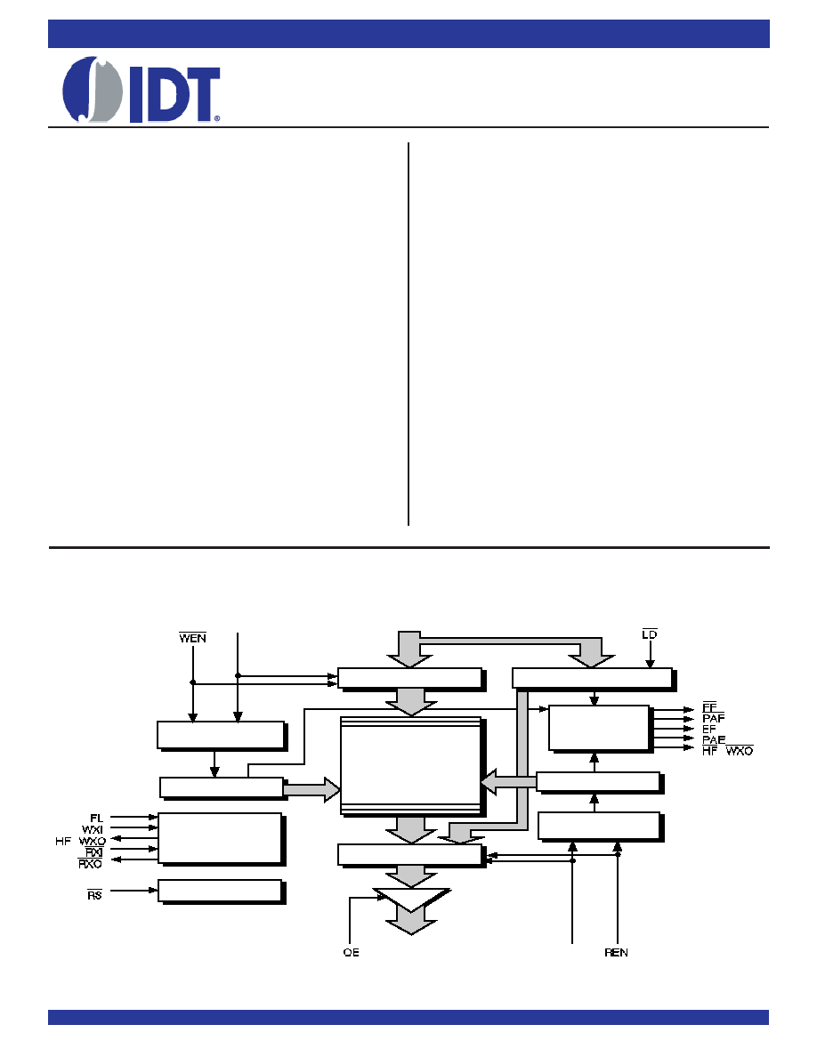
FUNCTIONAL BLOCK DIAGRAM
INPUT REGISTER
OUTPUT REGISTER
RAM ARRAY
256 x 18, 512 x 18
1,024 x 18, 2,048 x 18
4,096 x 18
OFFSET REGISTER
FLAG
LOGIC
/(
)
READ POINTER
READ CONTROL
LOGIC
WRITE CONTROL
LOGIC
WRITE POINTER
EXPANSION LOGIC
RESET LOGIC
WCLK
D0-D17
(
)/
RCLK
Q0-Q17
2766 drw 01
write controls. These FIFOs are applicable for a wide variety of data buffering
needs, such as optical disk controllers, Local Area Networks (LANs), and
interprocessorcommunication.
These FIFOs have 18-bit input and output ports. The input port is controlled
by a free-running clock (WCLK), and an input enable pin (
WEN). Data is read
into the synchronous FIFO on every clock when
WENisasserted.Theoutput
port is controlled by another clock pin (RCLK) and another enable pin (
REN).
The read clock can be tied to the write clock for single clock operation or the
two clocks can run asynchronous of one another for dual-clock operation. An
Output Enable pin (
OE) is provided on the read port for three-state control of
the output.
The synchronous FIFOs have two fixed flags, Empty (
EF) and Full (FF),
andtwoprogrammableflags,Almost-Empty(
PAE)andAlmost-Full(PAF).The
offsetloadingoftheprogrammableflagsiscontrolledbyasimplestatemachine,
and is initiated by asserting the Load pin (
LD). AHalf-Fullflag(HF)isavailable
when the FIFO is used in a single device configuration.
These devices are depth expandable using a Daisy-Chain technique. The
XI and XO pins are used to expand the FIFOs. In depth expansion configu-
ration, First Load (
FL) is grounded on the first device and set to HIGH for all
other devices in the Daisy Chain.
The IDT72205LB/72215LB/72225LB/72235LB/72245LB is fabricated
using IDT’s high-speed submicron CMOS technology.
相關(guān)PDF資料 |
PDF描述 |
|---|---|
| 723-611/019-000 | 15 A, MODULAR TERMINAL BLOCK, 1 ROW, 1 DECK |
| 72346-001LF | 20 CONTACT(S), FEMALE, STRAIGHT TELECOM AND DATACOM CONNECTOR, SOLDER, RECEPTACLE |
| 72346-001 | 20 CONTACT(S), FEMALE, STRAIGHT TELECOM AND DATACOM CONNECTOR, SOLDER, RECEPTACLE |
| 72346-002LF | 20 CONTACT(S), FEMALE, STRAIGHT TELECOM AND DATACOM CONNECTOR, SOLDER, RECEPTACLE |
| 723631L15PF9 | 512 X 36 OTHER FIFO, 11 ns, PQFP120 |
相關(guān)代理商/技術(shù)參數(shù) |
參數(shù)描述 |
|---|---|
| 72225LB25TFI | 制造商:Integrated Device Technology Inc 功能描述:FIFO Mem Sync Dual Depth/Width Uni-Dir 1K x 18 64-Pin STQFP 制造商:Integrated Device Technology Inc 功能描述:FIFO SYNC DUAL DEPTH/WIDTH UNI-DIR 1KX18 64TQFP - Rail/Tube |
| 72225LB25TFI8 | 制造商:Integrated Device Technology Inc 功能描述:FIFO Mem Sync Dual Depth/Width Uni-Dir 1K x 18 64-Pin STQFP T/R 制造商:Integrated Device Technology Inc 功能描述:FIFO SYNC DUAL DEPTH/WIDTH UNI-DIR 1KX18 64TQFP - Tape and Reel |
| 72226 | 制造商:Molex 功能描述: |
| 722-26 | 功能描述:高頻/射頻繼電器 26V DC-1GHz .15W RoHS:否 制造商:Omron Electronics 觸點(diǎn)形式:2 Form C (DPDT-BM) 觸點(diǎn)電流額定值: 線圈電壓:5 VDC 線圈類型:Non-Latching 頻率: 功耗:100 mW 端接類型:Solder Terminal 絕緣:20 dB to 30 dB at 1 GHz 介入損耗:0.2 dB at 1 GHz |
| 722-26/G | 制造商:Teledyne Relays 功能描述:EM RLY DPDT 1ADC/0.25AAC 26.5VDC 2KOHM TH - Bulk |
發(fā)布緊急采購(gòu),3分鐘左右您將得到回復(fù)。