- 您現(xiàn)在的位置:買賣IC網(wǎng) > PDF目錄369267 > 7211AI (Texas Instruments, Inc.) CMOS COMPARATORS WITH RAIL-TO-RAIL INPUT AND PUSH-PULL OUTPUT PDF資料下載
參數(shù)資料
| 型號(hào): | 7211AI |
| 廠商: | Texas Instruments, Inc. |
| 英文描述: | CMOS COMPARATORS WITH RAIL-TO-RAIL INPUT AND PUSH-PULL OUTPUT |
| 中文描述: | CMOS比較與軌到軌輸入和推挽輸出 |
| 文件頁(yè)數(shù): | 1/16頁(yè) |
| 文件大?。?/td> | 462K |
| 代理商: | 7211AI |
當(dāng)前第1頁(yè)第2頁(yè)第3頁(yè)第4頁(yè)第5頁(yè)第6頁(yè)第7頁(yè)第8頁(yè)第9頁(yè)第10頁(yè)第11頁(yè)第12頁(yè)第13頁(yè)第14頁(yè)第15頁(yè)第16頁(yè)
www.ti.com
FEATURES
Parameters Specified at 2.7-V, 5-V, and 15-V
Supplies
Supply Current 7
μ
A (Typ) at 5 V
Response Time 4
μ
s (Typ) at 5 V
Push-Pull Output
Input Common-Mode Range Beyond
V
CC–
and V
CC+
Low Input Current
APPLICATIONS
Battery-Powered Products
Notebooks and PDAs
Mobile Communications
Alarm and Security Circuits
Direct Sensor Interface
Replaces Amplifiers Used as Comparators
With Better Performance and Lower Current
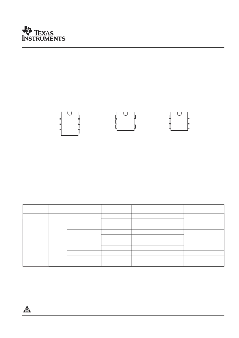
D PACKAGE
(TOPVIEW)
1
2
3
4
8
7
6
5
NC
V
CC+
OUT
NC
NC
IN–
IN+
V
CC–
NC – No internal connection
DBV PACKAGE
(TOPVIEW)
1
2
3
5
4
OUT
V
CC+
IN+
V
CC–
IN–
DCK PACKAGE
(TOPVIEW)
1
2
3
6
5
4
OUT
V
CC+
IN+
NC
V
CC–
IN–
DESCRIPTION/ORDERING INFORMATION
The TLV7211 and TLV7211A are micropower CMOS comparators available in the space-saving SOT-23-5
package. This makes the comparators ideal for space- and weight-critical designs. The TLV7211A features an
input offset voltage of 5 mV, and the TLV7211 features an input offset voltage of 15 mV.
TLV7211, TLV7211A
CMOS COMPARATORS
WITH RAIL-TO-RAIL INPUT AND PUSH-PULL OUTPUT
SLCS149B–AUGUST 2006–REVISED JANUARY 2007
The main benefits of the SOT-23-5 package are most apparent in small portable electronic devices, such as
mobile phones, pagers, notebook computers, personal digital assistants, and PCMCIA cards. The rail-to-rail
input voltage makes the TLV7211 or TLV7211A a good choice for sensor interfacing, such as light detector
circuits, optical and magnetic sensors, and alarm and status circuits.
The SOT-23-5 package's small size allows it to fit into tight spaces on PC boards.
ORDERING INFORMATION
V
(MAX)
T
A
PACKAGE
(1)
ORDERABLE PART NUMBER
TOP-SIDE MARKING
(2)
Reel of 2500
Tube of 75
Reel of 3000
Reel of 3000
Reel of 250
Reel of 2500
Tube of 75
Reel of 3000
Reel of 3000
Reel of 250
TLV7211AIDR
TLV7211AID
TLV7211AIDBVR
TLV7211AIDCKR
TLV7211AIDCKT
TLV7211IDR
TLV7211ID
TLV7211IDBVR
TLV7211IDCKR
TLV7211IDCKT
SOIC – D
7211AI
5 mV
SOT-23-5 – DBV
YBN_
SOT (SC-70) – DCK
Y8_
–40
°
C to 85
°
C
SOIC – D
TY7211
15 mV
SOT-23-5 – DBV
YBK_
SOT (SC-70) – DCK
Y7_
(1)
Package drawings, standard packing quantities, thermal data, symbolization, and PCB design guidelines are available at
www.ti.com/sc/package.
DBV/DCK: The actual top-side marking has one additional character that designates the assembly/test site.
(2)
Please be aware that an important notice concerning availability, standard warranty, and use in critical applications of Texas
Instruments semiconductor products and disclaimers thereto appears at the end of this data sheet.
PRODUCTION DATA information is current as of publication date.
Products conform to specifications per the terms of the Texas
Instruments standard warranty. Production processing does not
necessarily include testing of all parameters.
Copyright 2006–2007, Texas Instruments Incorporated
相關(guān)PDF資料 |
PDF描述 |
|---|---|
| 72173 | Complementary 30-V (D-S) MOSFET |
| 72231 | Dual P-Channel 12-V (D-S) MOSFET |
| 722560-1 | Ultra-Precision Operational Amplifier; Package: SOIC; No of Pins: 8; Temperature Range: Industrial |
| 722561-1 | Ultra-Precision Operational Amplifier; Package: SOIC; No of Pins: 8; Temperature Range: Industrial |
| 724663-1 | Ultra-Precision Operational Amplifier; Package: SOIC; No of Pins: 8; Temperature Range: Industrial |
相關(guān)代理商/技術(shù)參數(shù) |
參數(shù)描述 |
|---|---|
| 7211-AL | 功能描述:安裝硬件 1/4 LNGTH 5/16 DIA ROUND THUMB NUT RoHS:否 制造商:Harwin 類型:SMT Cable Clip 材料:Phosphor Bronze 安裝孔大小: 長(zhǎng)度:5 mm 外徑: 內(nèi)徑: 厚度: 電鍍:Tin 螺紋大小: |
| 7211B110195 | 制造商: 功能描述: 制造商:undefined 功能描述: |
| 7211BB-1 | 功能描述:沖壓機(jī)與沖模 PUNCH UNIT RD 1" RoHS:否 制造商:Souriau 大小: 產(chǎn)品:Dies 類型:Crimping 描述/功能: |
| 7211BB-1/2 | 功能描述:沖壓機(jī)與沖模 PUNCH UNIT RD 1/2" RoHS:否 制造商:Souriau 大小: 產(chǎn)品:Dies 類型:Crimping 描述/功能: |
| 7211BB-1-1/2 | 功能描述:沖壓機(jī)與沖模 PUNCH UNIT RD 1-1/2" RoHS:否 制造商:Souriau 大小: 產(chǎn)品:Dies 類型:Crimping 描述/功能: |
發(fā)布緊急采購(gòu),3分鐘左右您將得到回復(fù)。