- 您現(xiàn)在的位置:買賣IC網(wǎng) > PDF目錄369227 > 66116-201B (MICROPAC INDUSTRIES INC) Single Channel Optocoupler Electrically Similar to 4N47-4N49 Coaxial or Bulkhead Mount packages PDF資料下載
參數(shù)資料
| 型號: | 66116-201B |
| 廠商: | MICROPAC INDUSTRIES INC |
| 元件分類: | 光電耦合器 |
| 英文描述: | Single Channel Optocoupler Electrically Similar to 4N47-4N49 Coaxial or Bulkhead Mount packages |
| 中文描述: | 1 CHANNEL TRANSISTOR OUTPUT OPTOCOUPLER |
| 封裝: | HERMETIC SEALED, METAL PACKAGE-5 |
| 文件頁數(shù): | 1/2頁 |
| 文件大?。?/td> | 87K |
| 代理商: | 66116-201B |
MICROPAC INDUSTRIES, INC.
OPTOELECTRONIC PRODUCTS DIVISION
725 E. Walnut St., Garland, TX 75040
(972) 272-3571
Fax (972) 487-6918
www.micropac.com
E-MAIL: optosales@micropac.com
3 - 12
Single Channel Optocoupler
66116
Electrically Similar to 4N47-4N49
Coaxial or Bulkhead Mount packages
Mii
OPTOELECTRONIC PRODUCTS
DIVISION
Features:
High reliability
Base lead provided for conventional transistor
biasing
Very high gain, high voltage transistor
Hermetically sealed for reliability and stability
Stability over wide temperature range
High voltage electrical isolation
Applications:
Line Receivers
Switchmode Power Supplies
Signal ground isolation
Process Control input/output isolation
DESCRIPTION
Very high gain optocoupler utilizing GaAIAs infrared LED optically coupled to an N-P-N silicon phototransistor packaged in a
hermetically sealed metal case. These devices can be tested to customer specifications, as well as to MIL-PRF-38534 H&K
quality levels.
*ABSOLUTE MAXIMUM RATINGS
Input to Output Voltage........................................................................................................................................................
±
1kV
Collector-Base Voltage...........................................................................................................................................................45V
Collector-Emitter Voltage (See Note 1)..................................................................................................................................40V
Emitter-Base Voltage................................................................................................................................................................7V
Input Diode Reverse Voltage....................................................................................................................................................2V
Input Diode Continuous Forward Current at (or below) 65°C Free-Air Temperature (see note 2)....................................40mA
Continuous Collector Current..............................................................................................................................................50mA
Peak Diode Current (See Note 3).............................................................................................................................................1A
Continuous Transistor Power Dissipation at (or below) 25°C Free-Air Temperature (see Note 4) ................................300mW
Operating Free-Air Temperature Range............................................................................................................-55°C to +125°C
Storage Temperature..........................................................................................................................................-65°C to +125°C
Lead Temperature (1/16” (1.6mm) from case for 10 seconds)..........................................................................................240°C
* JEDEC registered data
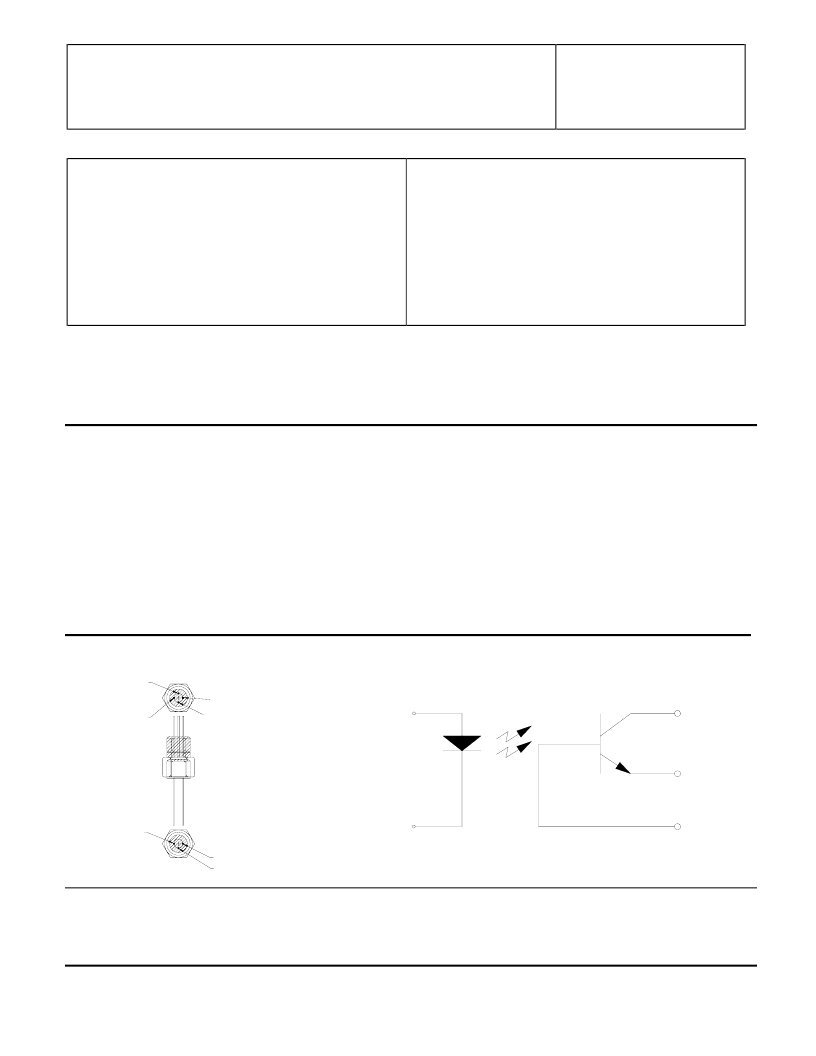
Package Dimensions Schematic Diagram
Base
Case Lead
Emitter
ANODE
CATHODE
Collector
Case Lead
E
B
K
C
A
Notes:
1. This value applies with the emitter-base diode open-circuited and the input-diode current equal to zero.
2. Derate linearly to 125°C free-air temperature at the rate of 0.67 mA/°C.
3. This value applies for t
w
≤
1us. PRR<300 pps.
4. Derate linearly to 125°C free-air temperature at the rate of 3 mW/°C.
相關(guān)PDF資料 |
PDF描述 |
|---|---|
| 66116-202 | Single Channel Optocoupler Electrically Similar to 4N47-4N49 Coaxial or Bulkhead Mount packages |
| 66116-202B | Single Channel Optocoupler Electrically Similar to 4N47-4N49 Coaxial or Bulkhead Mount packages |
| 66116-203 | Single Channel Optocoupler Electrically Similar to 4N47-4N49 Coaxial or Bulkhead Mount packages |
| 66116-203B | Single Channel Optocoupler Electrically Similar to 4N47-4N49 Coaxial or Bulkhead Mount packages |
| 66126-001 | SINGLE/DUAL CHANNEL, HERMETICALLY SEALED OPTOCOUPLER, SIMILAR TO 4N55 |
相關(guān)代理商/技術(shù)參數(shù) |
參數(shù)描述 |
|---|---|
| 66116-202 | 制造商:MII 制造商全稱:MII 功能描述:Single Channel Optocoupler Electrically Similar to 4N47-4N49 Coaxial or Bulkhead Mount packages |
| 66116-202B | 制造商:MII 制造商全稱:MII 功能描述:Single Channel Optocoupler Electrically Similar to 4N47-4N49 Coaxial or Bulkhead Mount packages |
| 66116-203 | 制造商:MII 制造商全稱:MII 功能描述:Single Channel Optocoupler Electrically Similar to 4N47-4N49 Coaxial or Bulkhead Mount packages |
| 66116-203B | 制造商:MII 制造商全稱:MII 功能描述:Single Channel Optocoupler Electrically Similar to 4N47-4N49 Coaxial or Bulkhead Mount packages |
| 661170-000 | 制造商:TE Connectivity 功能描述:Labels Thermal Transfer Printable Label Polyester Matte Yellow 76.2x30480mm |
發(fā)布緊急采購,3分鐘左右您將得到回復(fù)。