- 您現(xiàn)在的位置:買(mǎi)賣(mài)IC網(wǎng) > PDF目錄116755 > 552AF000108BG (SILICON LABORATORIES) VCXO, CLOCK, 693.48299 MHz, LVPECL OUTPUT PDF資料下載
參數(shù)資料
| 型號(hào): | 552AF000108BG |
| 廠商: | SILICON LABORATORIES |
| 元件分類(lèi): | VCXO, clock |
| 英文描述: | VCXO, CLOCK, 693.48299 MHz, LVPECL OUTPUT |
| 封裝: | ROHS COMPLIANT, SMD, 6 PIN |
| 文件頁(yè)數(shù): | 67/80頁(yè) |
| 文件大小: | 3734K |
| 代理商: | 552AF000108BG |
第1頁(yè)第2頁(yè)第3頁(yè)第4頁(yè)第5頁(yè)第6頁(yè)第7頁(yè)第8頁(yè)第9頁(yè)第10頁(yè)第11頁(yè)第12頁(yè)第13頁(yè)第14頁(yè)第15頁(yè)第16頁(yè)第17頁(yè)第18頁(yè)第19頁(yè)第20頁(yè)第21頁(yè)第22頁(yè)第23頁(yè)第24頁(yè)第25頁(yè)第26頁(yè)第27頁(yè)第28頁(yè)第29頁(yè)第30頁(yè)第31頁(yè)第32頁(yè)第33頁(yè)第34頁(yè)第35頁(yè)第36頁(yè)第37頁(yè)第38頁(yè)第39頁(yè)第40頁(yè)第41頁(yè)第42頁(yè)第43頁(yè)第44頁(yè)第45頁(yè)第46頁(yè)第47頁(yè)第48頁(yè)第49頁(yè)第50頁(yè)第51頁(yè)第52頁(yè)第53頁(yè)第54頁(yè)第55頁(yè)第56頁(yè)第57頁(yè)第58頁(yè)第59頁(yè)第60頁(yè)第61頁(yè)第62頁(yè)第63頁(yè)第64頁(yè)第65頁(yè)第66頁(yè)當(dāng)前第67頁(yè)第68頁(yè)第69頁(yè)第70頁(yè)第71頁(yè)第72頁(yè)第73頁(yè)第74頁(yè)第75頁(yè)第76頁(yè)第77頁(yè)第78頁(yè)第79頁(yè)第80頁(yè)
Si552
Rev. 0.5
7
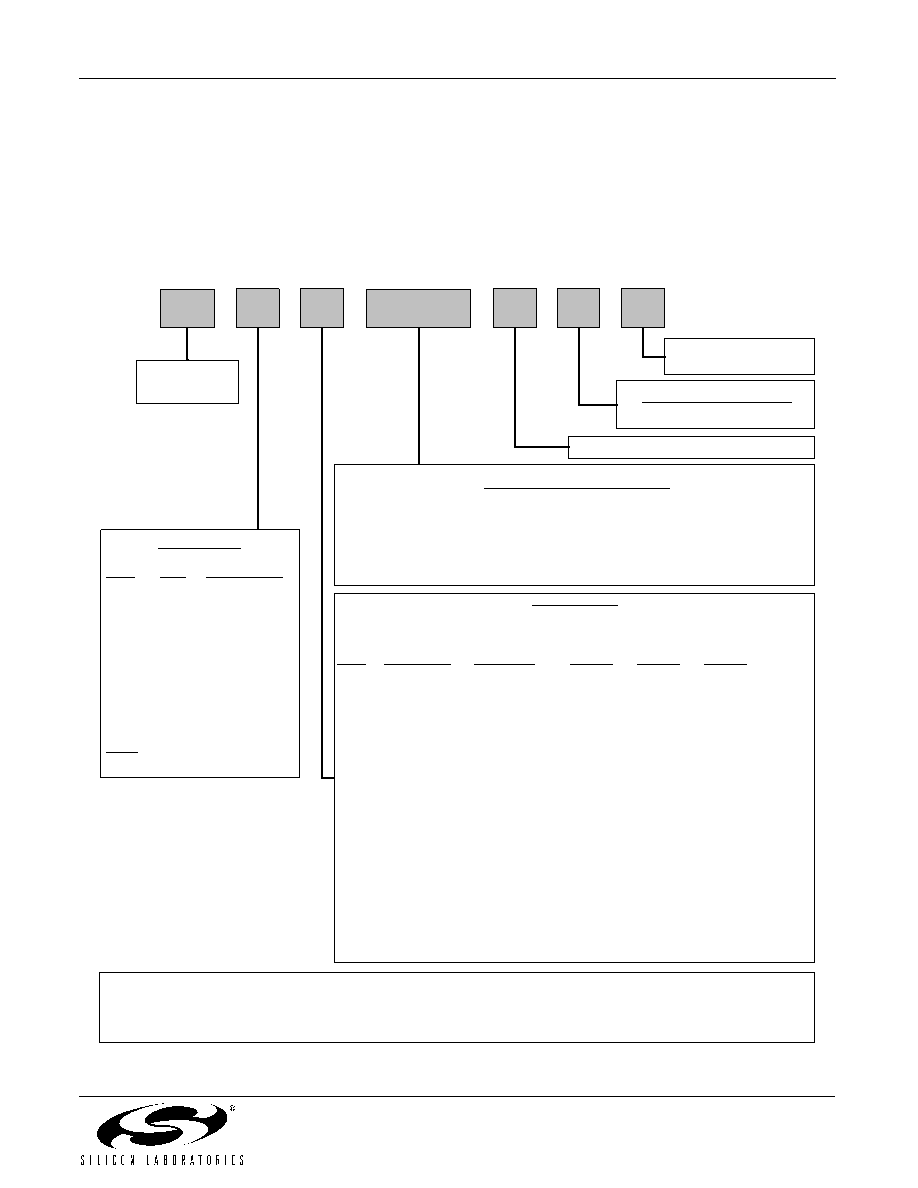
3. Ordering Information
The Si552 was designed to support a variety of options including frequency, temperature stability, tuning slope,
output format, and VDD.
Specific device configurations are programmed into the Si552 at time of shipment.
Configurations are specified using the Part Number Configuration chart shown below. Silicon Labs provides a web
browser-based
part
number
configuration
utility
to
simplify
this
process.
Refer
to
www.silabs.com/VCXOPartNumber to access this tool and for further ordering instructions. The Si552 VCXO
series is supplied in an industry-standard, RoHS compliant, lead-free, 6-pad, 5 x 7 mm package. Tape and reel
packaging is an ordering option.
Figure 1. Part Number Convention
Example Part Number: 552AF000108BGR is a 5 x 7 mm Dual VCXO in a 6 pad package. Since the six digit code (000108) is >
000100, f0 is 644.53125 MHz (lower frequency) and f1 is 693.48299 (higher frequency), with a 3.3 V supply and LVPECL output.
Temperature stability is specified as ±50 ppm and the tuning slope is 135 ppm/V. The part is specified for a –40 to +85 C° ambient
temperature range operation and is shipped in tape and reel format.
DD
R = Tape & Reel
Blank = Trays
Operating Temp Range (°C)
G
–40 to +85 °C
Device Revision Letter
2nd Option Code
Temperature
Tuning Slope
Minimum APR
Stability
Kv
(±ppm)
Code
± ppm (max)
ppm/V (typ)
@ 3.3 V
@ 2.5 V
@ 1.8 V
A
100
180
100
75
25
B
100
90
30
Note 6
C
50
180
150
125
75
D
509080
30
25
E
20
45
25
Note 6
F
50
135
100
75
50
Notes:
1. For best jitter and phase noise performance, always choose the smallest Kv that meets
the application’s minimum APR requirements. Unlike SAW-based solutions which
require higher higher Kv values to account for their higher temperature dependence,
the Si55x series provides lower Kv options to minimize noise coupling and jitter in real-
world PLL designs. See AN255 and AN266 for more information.
2. APR is the ability of a VCXO to track a signal over the product lifetime. A VCXO with an
APR of ±25 ppm is able to lock to a clock with a ±25 ppm stability, over 15 years.
3. Nominal Pull range (±) = 0.5 x VDD x tuning slope.
4. Nominal Absolute Pull Range (±APR) = Pull range – stability – lifetime aging
=0.5 x VDD x tuning slope – stability – 10 ppm
5. Minimum APR values noted above include worst case values for all parameters.
6. Combination not available.
552 Dual VCXO
Product Family
1st Option Code
Code
VDD
Output Format
A
3.3
LVPECL
B3.3
LVDS
C3.3
CMOS
D3.3
CML
E
2.5
LVPECL
F2.5
LVDS
G2.5
CMOS
H2.5
CML
J1.8
CMOS
K1.8
CML
Notes:
CMOS available to 160 MHz.
6-digit Frequency Designator Code
Two unique frequencies can be specified within the following bands of frequencies: 10 to
945 MHz, 970 to 1134 MHz, and 1213 to 1417 MHz. A six digit code will be assigned for
the specified combination of frequencies. Codes > 000100 refer to dual XOs programmed
with the lower frequency value selected when FS = 0, and the higher value when FS = 1.
Six digit codes < 000100 refer to dual XOs programmed with the higher frequency value
selected when FS = 0, and the lower value when FS = 1.
552
X
XXXXXX
B
G
R
相關(guān)PDF資料 |
PDF描述 |
|---|---|
| 552AF000127BGR | VCXO, CLOCK, 693.48299 MHz, LVPECL OUTPUT |
| 552BA000121BGR | VCXO, CLOCK, 666.51429 MHz, LVDS OUTPUT |
| 552BC000112BG | VCXO, CLOCK, 644.53125 MHz, LVDS OUTPUT |
| 552BC000118BG | VCXO, CLOCK, 74.25 MHz, LVDS OUTPUT |
| 550DD173M371BGR | VCXO, CLOCK, 173.371 MHz, CMOS/TTL OUTPUT |
相關(guān)代理商/技術(shù)參數(shù) |
參數(shù)描述 |
|---|---|
| 552AF000147DGR | 制造商:Silicon Laboratories Inc 功能描述:DUAL VCXO, LVPECL, 3.3V - Tape and Reel |
| 552AF000177DG | 制造商:Silicon Laboratories Inc 功能描述:DUAL VCXO, LVPECL, 3.3V - Trays |
| 552AF000177DGR | 制造商:Silicon Laboratories Inc 功能描述:DUAL VCXO, LVPECL, 3.3V - Tape and Reel |
| 552AF000207DG | 制造商:Silicon Laboratories Inc 功能描述: |
| 552AF000207DGR | 制造商:Silicon Laboratories 功能描述:Controlled Oscillator 622.08MHz/625MHz VCXO LVPECL 6-Pin SMD T/R |
發(fā)布緊急采購(gòu),3分鐘左右您將得到回復(fù)。