- 您現(xiàn)在的位置:買賣IC網(wǎng) > PDF目錄157230 > 54AC10 (National Semiconductor Corporation) Triple 3-Input NAND Gate PDF資料下載
參數(shù)資料
| 型號: | 54AC10 |
| 廠商: | National Semiconductor Corporation |
| 英文描述: | Triple 3-Input NAND Gate |
| 中文描述: | 三3輸入與非門 |
| 文件頁數(shù): | 2/6頁 |
| 文件大小: | 110K |
| 代理商: | 54AC10 |
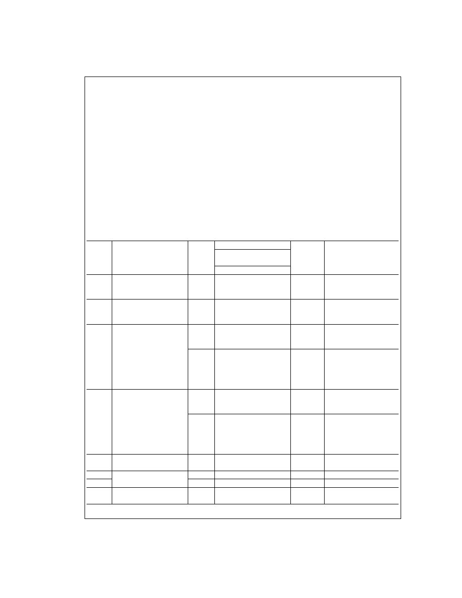
Absolute Maximum Ratings (Note 1)
If Military/Aerospace specified devices are required,
please contact the National Semiconductor Sales Office/
Distributors for availability and specifications.
Supply Voltage (V
CC)
0.5V to +7.0V
DC Input Diode Current (I
IK)
V
I = 0.5V
20 mA
V
I = VCC + 0.5V
+20 mA
DC Input Voltage (V
I)
0.5V to V
CC + 0.5V
DC Output Diode Current (I
OK)
V
O = 0.5V
20 mA
V
O = VCC + 0.5V
+20 mA
DC Output Voltage (V
O)
0.5V to V
CC + 0.5V
DC Output Source
or Sink Current (I
O)
±50 mA
DC V
CC or Ground Current
per Output Pin (I
CC or IGND)
±50 mA
Storage Temperature (T
STG)
65C to +150C
Junction Temperature (T
J)
CDIP
175C
Recommended Operating
Conditions
Supply Voltage (V
CC)
’AC
2.0V to 6.0V
Input Voltage (V
I)
0VtoV
CC
Output Voltage (V
O)
0VtoV
CC
Operating Temperature (T
A)
54AC
55C to +125C
Minimum Input Edge Rate (
V/t)
’AC Devices
V
IN from 30% to 70% of VCC
V
CC @ 3.3V, 4.5V, 5.5V
125 mV/ns
Note 1: Absolute maximum ratings are those values beyond which damage
to the device may occur. The databook specifications should be met, without
exception, to ensure that the system design is reliable over its power supply,
temperature, and output/input loading variables. National does not recom-
mend operation of FACT circuits outside databook specifications.
DC Characteristics for ’AC Family Devices
54AC
Symbol
Parameter
V
CC
T
A =
Units
Conditions
(V)
55C to +125C
Guaranteed Limits
V
IH
Minimum High Level
3.0
2.1
V
OUT = 0.1V
Input Voltage
4.5
3.15
V
or V
CC 0.1V
5.5
3.85
V
IL
Maximum Low Level
3.0
0.9
V
OUT = 0.1V
Input Voltage
4.5
1.35
V
or V
CC 0.1V
5.5
1.65
V
OH
Minimum High Level
3.0
2.9
I
OUT = 50 A
Output Voltage
4.5
4.4
V
5.5
5.4
(Note 2)
V
IN = VIL or VIH
3.0
2.4
I
OH = 12 mA
4.5
3.7
V
I
OH = 24 mA
5.5
4.7
I
OH = 24 mA
V
OL
Maximum Low Level
3.0
0.1
I
OUT = 50 A
Output Voltage
4.5
0.1
V
5.5
0.1
(Note 2)
V
IN = VIL or VIH
3.0
0.5
I
OL =12mA
4.5
0.5
V
I
OL =24mA
5.5
0.5
I
OL =24mA
I
IN
Maximum Input
5.5
±1.0
A
V
I = VCC, GND
I
OLD
Minimum Dynamic
Output Current (Note 3)
5.5
50
mA
V
OLD = 1.65V Max
I
OHD
5.5
50
mA
V
OHD = 3.85V Min
I
CC
Maximum Quiescent
5.5
40.0
A
V
IN =VCC
Supply Current
or GND
Note 2: All outputs loaded; thresholds on input associated with output under test.
www.national.com
2
相關PDF資料 |
PDF描述 |
|---|---|
| 54AC10D | Triple 3-Input NAND Gate |
| 54AC10F | Triple 3-Input NAND Gate |
| 54AC10L | Triple 3-Input NAND Gate |
| 54AC74FM | AC SERIES, DUAL POSITIVE EDGE TRIGGERED D FLIP-FLOP, COMPLEMENTARY OUTPUT, CDFP14 |
| 54ACQ240DMQB | AC SERIES, DUAL 4-BIT DRIVER, INVERTED OUTPUT, CDIP20 |
相關代理商/技術參數(shù) |
參數(shù)描述 |
|---|---|
| 54AC1010DM | 制造商:未知廠家 制造商全稱:未知廠家 功能描述:Logic IC |
| 54AC1016DM | 制造商:未知廠家 制造商全稱:未知廠家 功能描述:Logic IC |
| 54AC1017DM | 制造商:未知廠家 制造商全稱:未知廠家 功能描述:Logic IC |
| 54AC109 | 制造商:NSC 制造商全稱:National Semiconductor 功能描述:Dual JK Positive Edge-Triggered Flip-Flop |
| 54AC109D | 制造商:NSC 制造商全稱:National Semiconductor 功能描述:Dual JK Positive Edge-Triggered Flip-Flop |
發(fā)布緊急采購,3分鐘左右您將得到回復。