- 您現(xiàn)在的位置:買(mǎi)賣(mài)IC網(wǎng) > PDF目錄360230 > 522923D Dual/Triple Ultra-Low-Voltage SOT23 µP Supervisory Circuits PDF資料下載
參數(shù)資料
| 型號(hào): | 522923D |
| 英文描述: | Dual/Triple Ultra-Low-Voltage SOT23 µP Supervisory Circuits |
| 中文描述: | 集成電路 |
| 文件頁(yè)數(shù): | 7/24頁(yè) |
| 文件大小: | 418K |
| 代理商: | 522923D |
第1頁(yè)第2頁(yè)第3頁(yè)第4頁(yè)第5頁(yè)第6頁(yè)當(dāng)前第7頁(yè)第8頁(yè)第9頁(yè)第10頁(yè)第11頁(yè)第12頁(yè)第13頁(yè)第14頁(yè)第15頁(yè)第16頁(yè)第17頁(yè)第18頁(yè)第19頁(yè)第20頁(yè)第21頁(yè)第22頁(yè)第23頁(yè)第24頁(yè)
7
LTC1286/LTC1298
TYPICAL PERFOR
M
A
CE CHARACTERISTICS
U
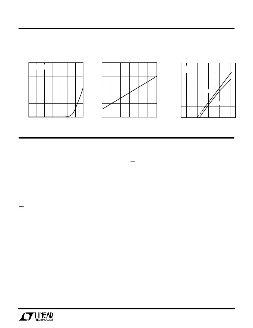
TEMPERATURE (°C)
–55
C
100
150
25
45
65
85
LT1286/98 G14
50
0
–35
–15
5
200
= V
REF
= 5V
SUPPLY VOLTAGE (V)
3
1
D
2
3
4
5
6
7
LTC 1286/98 G17
8
9
T
A
= 25°C
TEMPERATURE (°C)
–60
L
1000
100
10
1
0.1
0.01
100
1196/98 G19
–20
20
60
140
–40
0
40
80
120
V
CC
= 5V
V
REF
= 5V
ON CHANNEL
OFF CHANNEL
Input Channel Leakage Current
vs Temperature
Digital Input Logic Threshold
vs Supply Voltage
Minimum Clock Frequency
for 0.1 LSB Error vs Temperature
PI
FU
CTIO
N
S
U
U
LTC1286
V
REF
(Pin 1):
Reference Input. The reference input defines
the span of the A/D converter.
IN
+
(Pin 2):
Positive Analog Input.
IN
–
(Pin 3):
Negative Analog Input.
GND (Pin 4):
Analog Ground. GND should be tied directly
to an analog ground plane.
CS/SHDN (Pin 5):
Chip Select Input. A logic low on this
input enables the LTC1286. A logic high on this input
disables and powers down the LTC1286.
D
OUT
(Pin 6):
Digital Data Output. The A/D conversion
result is shifted out of this output.
CLK (Pin 7):
Shift Clock. This clock synchronizes the serial
data transfer and determines conversion speed.
V
CC
(Pin 8):
Power Supply Voltage. This pin provides
power to the A/D converter. It must be kept free of noise
and ripple by bypassing directly to the analog ground
plane.
LTC1298
CS/SHDN (Pin 1):
Chip Select Input. A logic low on this
input enables the LTC1298. A logic high on this input
disables and powers down the LTC1298.
CH0 (Pin 2):
Analog Input.
CH1 (Pin 3):
Analog Input.
GND (Pin 4):
Analog Ground. GND should be tied directly
to an analog ground plane.
D
IN
(Pin 5):
Digital Data Input. The multiplexer address is
shifted into this input.
D
OUT
(Pin 6):
Digital Data Output. The A/D conversion
result is shifted out of this output.
CLK (Pin 7):
Shift Clock. This clock synchronizes the
serial data transfer and determines conversion speed.
V
CC
/V
REF
(Pin 8):
Power Supply and Reference Voltage.
This pin provides power and defines the span of the A/D
converter. It must be kept free of noise and ripple by
bypassing directly to the analog ground plane.
相關(guān)PDF資料 |
PDF描述 |
|---|---|
| 522929C | IC |
| 522946A | Dual/Triple Ultra-Low-Voltage SOT23 µP Supervisory Circuits |
| 522925X | IC |
| 52602499 | LOETSTATION WECP 82 |
| 52610-1090 | Dual/Triple Ultra-Low-Voltage SOT23 µP Supervisory Circuits |
相關(guān)代理商/技術(shù)參數(shù) |
參數(shù)描述 |
|---|---|
| 5229-24CPB | 制造商:MOLEX 制造商全稱(chēng):Molex Electronics Ltd. 功能描述:2.54mm (.100) Vertical, Non-ZIF, Low Profile Receptacle, 24 Circuits |
| 522925-000 | 制造商:TE Connectivity 功能描述:Shrink Boot Adapters 180° 制造商:TE Connectivity 功能描述:TXR40AB00-2012CI - Bulk |
| 5229-25APB | 制造商:MOLEX 制造商全稱(chēng):Molex Electronics Ltd. 功能描述:2.54mm (.100) Right Angle, Non-ZIF, Low Profile Receptacle, 25 Circuits |
| 5229-25CPB | 制造商:MOLEX 制造商全稱(chēng):Molex Electronics Ltd. 功能描述:2.54mm (.100) Vertical, Non-ZIF, Low Profile Receptacle, 25 Circuits |
| 522925X | 制造商:未知廠(chǎng)家 制造商全稱(chēng):未知廠(chǎng)家 功能描述:IC |
發(fā)布緊急采購(gòu),3分鐘左右您將得到回復(fù)。