- 您現(xiàn)在的位置:買賣IC網(wǎng) > PDF目錄371554 > 2SK3341-01 (FUJI ELECTRIC CO LTD) N-CHANNEL SILICON POWER MOS-FET PDF資料下載
參數(shù)資料
| 型號: | 2SK3341-01 |
| 廠商: | FUJI ELECTRIC CO LTD |
| 元件分類: | JFETs |
| 英文描述: | N-CHANNEL SILICON POWER MOS-FET |
| 中文描述: | 10 A, 900 V, 1.2 ohm, N-CHANNEL, Si, POWER, MOSFET, TO-247 |
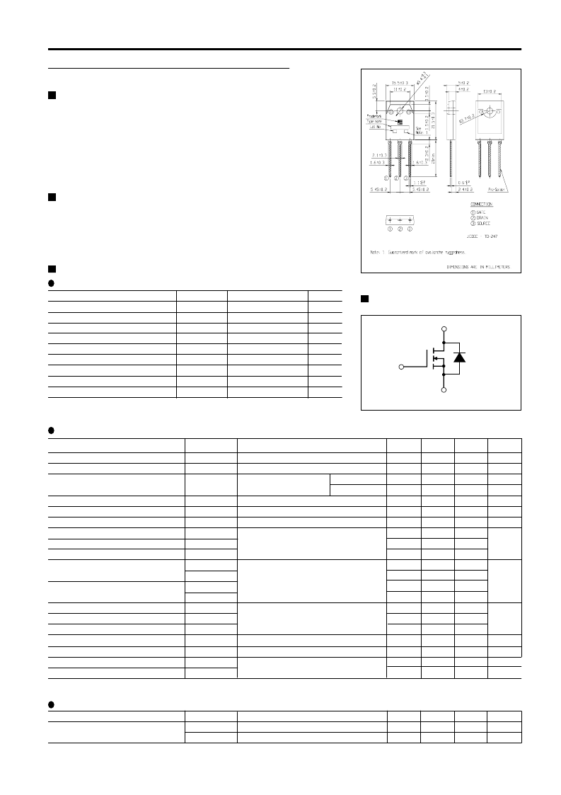
| 封裝: | TO-247, 3 PIN |
| 文件頁數(shù): | 1/4頁 |
| 文件大?。?/td> | 105K |
| 代理商: | 2SK3341-01 |
1
Item
Drain-source voltage
Continuous drain current
Pulsed drain current
Gate-source voltage
Repetitive or non-repetitive
Maximum Avalanche Energy
Max. power dissipation
Operating and storage
temperature range
Symbol
V
DS
I
D
I
D(puls]
V
GS
I
AR *2
E
AV *1
P
D
T
ch
T
stg
Rating
900
±10
±40
±30
Unit
V
A
A
V
A
mJ
W
°C
10
648
310
+150
-55 to +150
Electrical characteristics (T
c
=25°C unless otherwise specified)
Thermalcharacteristics
2SK3341-01
N-CHANNEL SILICON POWER MOS-FET
FUJI POWER MOS-FET
Features
High speed switching
Low on-resistance
No secondary breadown
Low driving power
Avalanche-proof
Applications
Switching regulators
UPS (Uninterruptible Power Supply)
DC-DC converters
Maximum ratings and characteristic
Absolute maximum ratings
(Tc=25°C unless otherwise specified)
Item
Symbol Test Conditions
R
th(ch-c)
channel to case
R
th(ch-a)
channel to ambient
Zero gate voltage drain current I
DSS
DS
=900V
V
ch
=25°C
V
GS
=0V T
ch
=125°C
=±30V
DS
=0V
V
GS
I
D
=5A V
GS
=10V
I
D
=5A V
DS
=25V
V
DS
=25V
V
GS
=0V
f=1MHz
V
CC
=600V I
D
=10A
V
GS
=10V
R
GS
=10
Min. Typ. Max. Units
900
2.5
3.0
10
0.2
10
0.92
3.5
7
2200
240
115
28
70
220
90
120
36
40
10
1.00
1.8
21.0
V
V
μA
mA
nA
S
pF
nC
A
V
μs
μC
ns
Min. Typ. Max. Units
Thermal resistance
0.403
50.0
°C/W
°C/W
Symbol
V
(BR)DSS
V
GS(th)
I
GSS
R
DS(on)
g
fs
C
iss
C
oss
C
rss
td
(on)
t
r
td
(off)
t
f
Q
G
Q
GS
Q
GD
I
AV
V
SD
t
rr
Q
rr
Item
Drain-source breakdown voltaget
Gate threshold voltage
Gate-source leakage current
Drain-source on-state resistance
Forward transcondutance
Input capacitance
Output capacitance
Reverse transfer capacitance
Turn-on time t
on
Turn-off time t
off
Total gate charge
Gate-Source charge
Gete-Drain charge
Avalanche capability
Diode forward on-voltage
Reverse recovery time
Reverse recovery charge
Test Conditions
I
D
=1mA V
GS
=0V
I
D
=1mA V
DS
=V
GS
Vcc=450V
I
D
=10A
V
GS
=10V
L=11.9mH T
ch
=25°C
I
F
=2xI
DR
V
GS
=0V T
ch
=25°C
I
F
=I
DR
V
GS
=0V
-dI
F
/dt=100A/μs T
ch
=25°C
*1 L=11.9mH, Vcc=90V *2 Tch<
3.5
500
1.0
100
1.2
3300
360
173
42
105
330
135
180
54
60
1.50
Equivalent circuit schematic
Gate(G)
Source(S)
Drain(D)
相關(guān)PDF資料 |
PDF描述 |
|---|---|
| 2SK3342 | CONTACT |
| 2SK334 | Silicon N-Channel Junction-Type Field Effect TR For CONDENSER MICROPHONES |
| 2SK3362 | POWER MOSFET |
| 2SK3362-01 | MOSFETs |
| 2SK3363-01 | N-CHANNEL SILICON POWER MOS-FET |
相關(guān)代理商/技術(shù)參數(shù) |
參數(shù)描述 |
|---|---|
| 2SK3341-01SC | 制造商:Fuji Electric 功能描述: |
| 2SK3342 | 制造商:TOSHIBA 制造商全稱:Toshiba Semiconductor 功能描述:TOSHIBA Field Effect Transistor Silicon N Channel MOS Type (MOSV) |
| 2SK3342(Q) | 制造商:Toshiba 功能描述:Bulk |
| 2SK3342(SMD) | 制造商:未知廠家 制造商全稱:未知廠家 功能描述:TRANSISTOR | MOSFET | N-CHANNEL | 250V V(BR)DSS | 4.5A I(D) | TO-252AA |
| 2SK3342(TE16L1,NQ) | 制造商:Toshiba America Electronic Components 功能描述:MOSFET N-CH 250V 4.5A PW-MOLD |
發(fā)布緊急采購,3分鐘左右您將得到回復(fù)。