- 您現(xiàn)在的位置:買賣IC網(wǎng) > PDF目錄371367 > 210007039-002 (Electronic Theatre Controls, Inc.) 350mWAudio Power Amplifier with Shutdown Mode PDF資料下載
參數(shù)資料
| 型號: | 210007039-002 |
| 廠商: | Electronic Theatre Controls, Inc. |
| 英文描述: | 350mWAudio Power Amplifier with Shutdown Mode |
| 中文描述: | 350mWAudio功率放大器關(guān)斷模式 |
| 文件頁數(shù): | 3/21頁 |
| 文件大小: | 877K |
| 代理商: | 210007039-002 |
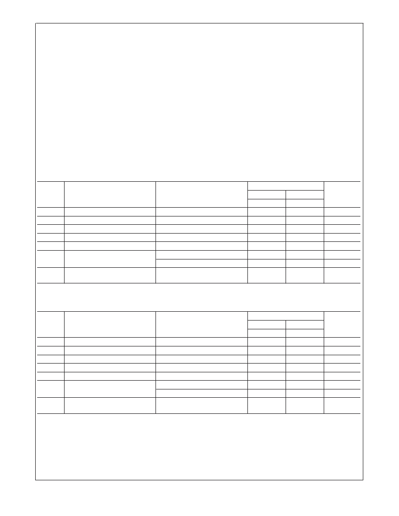
Absolute Maximum Ratings
(Notes 2, 3)
If Military/Aerospace specified devices are required,
please contact the
CSMSC
Semiconductor Sales Office/
Distributors for availability and specifications.
Supply Voltage
Storage Temperature
Input Voltage
Power Dissipation (P
D
) (Note 4)
ESD Susceptibility (Note 5)
ESD Susceptibility (Note 6)
Junction Temperature (T
J
)
Soldering Information (Note 1)
Small Outline Package
Vapor Phase (60 seconds)
6.0V
65C to +150C
0.3V to V
DD
+0.3V
Internally Limited
3.5kV
250V
150C
215C
Infrared (15 seconds)
Thermal Resistance
θ
JC
(MSOP)
θ
JA
(MSOP)
θ
JC
(SOP)
θ
JA
(SOP)
θ
JA
(LLP)
θ
JA
(LLP)
220C
56C/W
210C/W
35C/W
170C/W
117C/W (Note 10)
150C/W (Note 11)
Operating Ratings
(Notes 2, 3)
Temperature Range
T
MIN
≤
T
A
≤
T
MAX
Supply Voltage
40C
≤
T
A
≤
85C
2.0V
≤
V
CC
≤
5.5V
Electrical Characteristics V
DD
= 5V
(Notes 2, 3)
The following specifications apply for V
DD
= 5V, R
L
= 16
unless otherwise stated. Limits apply for T
A
= 25C.
Symbol
Parameter
Conditions
HWD21
19
Units
(Limits)
Typical
(Note 7)
1.5
1.0
Limit
(Notes 8, 9)
3.0
5.0
4.0
1.0
50
I
DD
I
SD
V
SDIH
V
SDIL
V
OS
Quiescent Power Supply Current
Shutdown Current
Shutdown Voltage Input High
Shutdown Voltage Input Low
Output Offset Voltage
V
IN
= 0V, I
o
= 0A
V
PIN1
= V
DD
(Note 12)
mA (max)
μA (max)
V (min)
V (max)
mV (max)
mW
mW
%
V
IN
= 0V
THD = 10%, f
IN
= 1kHz
THD = 10%, f
IN
= 1kHz, R
L
= 8
P
O
= 270mW
RMS
, A
VD
= 2, f
IN
=
1kHz
5
P
O
Output Power
350
300
1
THD+N
Total Harmonic Distortion + Noise
Electrical Characteristics V
DD
= 3V
(Notes 2, 3)
The following specifications apply for V
DD
= 3V and R
L
= 16
load unless otherwise stated. Limits apply to T
A
= 25C.
Symbol
Parameter
Conditions
HWD21
19
Units
(Limits)
Typical
(Note 7)
1.0
0.7
Limit
(Notes 8, 9)
3.0
5.0
2.4
0.6
50
I
DD
I
SD
V
SDIH
V
SDIL
V
OS
Quiescent Power Supply Current
Shutdown Current
Shutdown Voltage Input High
Shutdown Voltage Input Low
Output Offset Voltage
V
IN
= 0V, I
o
= 0A
V
PIN1
= V
DD
(Note 12)
mA (max)
μA (max)
V (min)
V (max)
mV
mW
mW
%
V
IN
= 0V
THD = 10%, f
IN
= 1kHz
THD = 10%, f
IN
= 1kHz, R
L
= 8
P
O
= 80mW
RMS
, A
VD
= 2, f
IN
=
1kHz
5
P
O
Output Power
110
90
1
THD+N
Total Harmonic Distortion + Noise
2
相關(guān)PDF資料 |
PDF描述 |
|---|---|
| 21001 | SICHERHEITSSCHALTER CADET 1N/C 1N/O |
| 21002 | SICHERHEITSSCHALTER CADET 2N/C |
| 21003 | SICHERHEITSSCHALTER CADETH 1N/C 1N/O |
| 21004 | SICHERHEITSSCHALTER CADET 2N/C |
| 21005 | SICHERHEITSSCHALTER MONTAGEPLATTE |
相關(guān)代理商/技術(shù)參數(shù) |
參數(shù)描述 |
|---|---|
| 2100-0790 | 制造商:Agilent Technologies 功能描述: 制造商:AGILNT 功能描述: |
| 2100-08 | 功能描述:沖壓機(jī)與沖模 RJ45 8 POSITION RoHS:否 制造商:Souriau 大小: 產(chǎn)品:Dies 類型:Crimping 描述/功能: |
| 2-100-080 | 制造商:Thomas & Betts 功能描述:Fittings Connector 1inch Aluminum |
| 21-00084 | 制造商: 功能描述: 制造商:undefined 功能描述: |
| 210009 | 制造商:NJSEMI 制造商全稱:New Jersey Semi-Conductor Products, Inc. 功能描述:Schottky Rectifiers |
發(fā)布緊急采購,3分鐘左右您將得到回復(fù)。