- 您現(xiàn)在的位置:買賣IC網(wǎng) > PDF目錄23096 > 0ICAH-002-XTP (ON SEMICONDUCTOR) DATACOM, INTERFACE CIRCUIT, PDSO8 PDF資料下載
參數(shù)資料
| 型號(hào): | 0ICAH-002-XTP |
| 廠商: | ON SEMICONDUCTOR |
| 元件分類: | 網(wǎng)絡(luò)接口 |
| 英文描述: | DATACOM, INTERFACE CIRCUIT, PDSO8 |
| 封裝: | 0.150 INCH, GREEN, PLASTIC, SOIC-8 |
| 文件頁數(shù): | 8/12頁 |
| 文件大小: | 501K |
| 代理商: | 0ICAH-002-XTP |
AMIS-42670 High-Speed CAN Transceiver
Data Sheet
For Long Networks
8.0 Electrical Characteristics
8.1 Definitions
All voltages are referenced to GND (pin 2). Positive currents flow into the IC. Sinking current means the current is flowing into the pin;
sourcing current means the current is flowing out of the pin.
8.2 Absolute Maximum Ratings
Stresses above those listed in the following table may cause permanent device failure. Exposure to absolute maximum ratings for
extended periods may affect device reliability.
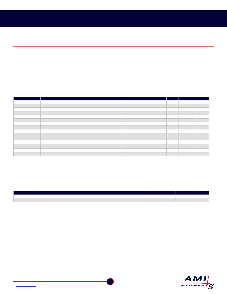
Table 4: Absolute Maximum Ratings
Symbol
Parameter
Conditions
Min.
Max.
Unit
VCC
Supply voltage
-0.3
+7
V
VCANH
DC voltage at pin CANH
0 < VCC < 5.25V; no time limit
-45
+45
V
VCANL
DC voltage at pin CANL
0 < VCC < 5.25V; no time limit
-45
+45
V
VTxD
DC voltage at pin TxD
-0.3
VCC + 0.3
V
VRxD
DC voltage at pin RxD
-0.3
VCC + 0.3
V
VS
DC voltage at pin S
-0.3
VCC + 0.3
V
VREF
DC voltage at pin VREF
-0.3
VCC + 0.3
V
Vtran(CANH)
Transient voltage at pin CANH
Note 1
-150
+150
V
Vtran(CANL)
Transient voltage at pin CANL
Note 1
-150
+150
V
Vesd
Electrostatic discharge voltage at all pins
Note 2
Note 4
-4
-750
+4
+750
kV
V
Latch-up
Static latch-up at all pins
Note 3
100
mA
Tstg
Storage temperature
-55
+155
°C
Tamb
Ambient temperature
-40
+125
°C
Tjunc
Maximum junction temperature
-40
+150
°C
Notes:
1.
Applied transient waveforms in accordance with ISO 7637 part 3, test pulses 1, 2, 3a, and 3b (see Figure 4).
2.
Standardized human body model ESD pulses in accordance to MIL883 method 3015.7.
3.
Static latch-up immunity: static latch-up protection level when tested according to EIA/JESD78.
4.
Standardized charged device model ESD pulses when tested according to EOS/ESD DS5.3-1993.
8.3 Thermal Characteristics
Table 5: Thermal Characteristics
Symbol
Parameter
Conditions
Value
Unit
Rth(vj-a)
Thermal resistance from junction to ambient in SO8 package
In free air
150
K/W
Rth(vj-s)
Thermal resistance from junction to substrate of bare die
In free air
45
K/W
5
AMI Semiconductor
– October 07, Rev. 1.0
www.amis.com Specifications subject to change without notice
相關(guān)PDF資料 |
PDF描述 |
|---|---|
| 0ICAW-001-XTD | DATACOM, INTERFACE CIRCUIT, PDSO20 |
| 0ICAW-001-XTP | DATACOM, INTERFACE CIRCUIT, PDSO20 |
| 0ICAW-001-XTD | DATACOM, INTERFACE CIRCUIT, PDSO20 |
| 0ICAW-001-XTP | DATACOM, INTERFACE CIRCUIT, PDSO20 |
| 0VA3AB1AA-019.44M | OCVCXO, CLOCK, 19.44 MHz, LVCMOS OUTPUT |
相關(guān)代理商/技術(shù)參數(shù) |
參數(shù)描述 |
|---|---|
| 0ICB533100A | 制造商:LG Corporation 功能描述:RYSTAL SEMICONDUCTOR CS5331A-KSR 8SOIC NS-PDP42/52 制造商:LG Corporation 功能描述:SUB ONLY IC- CRYSTAL SEMICONDU CS5331A-KSR 4.75TO5 |
| 0ICB533100B | 制造商:LG Corporation 功能描述:IC,A/D Converter |
| 0ICB841500B | 制造商:LG Corporation 功能描述:IC,CRYSTAL SEMICONDU |
| 0ICB841500D | 制造商:LG Corporation 功能描述:IC,CRYSTAL SEMICONDU |
| 0ICB841500E | 制造商:LG Corporation 功能描述:IC,Receiver |
發(fā)布緊急采購,3分鐘左右您將得到回復(fù)。