- 您現(xiàn)在的位置:買賣IC網(wǎng) > PDF目錄24947 > 08F1644 TRANSISTOR MOSFET D-PAK PDF資料下載
參數(shù)資料
| 型號(hào): | 08F1644 |
| 英文描述: | TRANSISTOR MOSFET D-PAK |
| 中文描述: | 晶體管MOSFET的的D - Pak |
| 文件頁數(shù): | 6/10頁 |
| 文件大小: | 252K |
| 代理商: | 08F1644 |
MTD5N25E
5
Motorola TMOS Power MOSFET Transistor Device Data
DRAIN–TO–SOURCE DIODE CHARACTERISTICS
Figure 8. Gate–To–Source and Drain–To–Source
Voltage versus Total Charge
Figure 9. Resistive Switching Time
Variation versus Gate Resistance
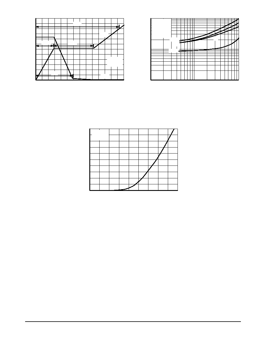
Figure 10. Diode Forward Voltage versus Current
RG, GATE RESISTANCE (OHMS)
1
10
100
1
t,
TIME
(ns)
tf
td(off)
td(on)
300
V
GS
,GA
TE–T
O–SOURCE
VOL
TAGE
(VOL
TS)
250
150
100
0
10
0
QT, TOTAL CHARGE (nC)
V
DS
,DRAIN–T
O–SOURCE
VOL
TAGE
(VOL
TS)
12
8
4
2
4
6
14
VDS
VGS
8
0
Q1
Q2
QT
Q3
10
tr
VDD = 125 V
ID = 5 A
VGS = 10 V
TJ = 25°C
ID = 5 A
TJ = 25°C
0.5
0.6
0.7
0.8
0.9
0
2
5
VSD, SOURCE–TO–DRAIN VOLTAGE (VOLTS)
I S
,SOURCE
CURRENT
(AMPS)
VGS = 0 V
TJ = 25°C
4
3
0.55
0.65
0.75
0.85
1
6
2
10
12
50
200
0.95
SAFE OPERATING AREA
The Forward Biased Safe Operating Area curves define the
maximum simultaneous drain–to–source voltage and drain
current that a transistor can handle safely when it is forward
biased. Curves are based upon maximum peak junction
temperature and a case temperature (TC) of 25
°C. Peak
repetitive pulsed power limits are determined by using the
thermal response data in conjunction with the procedures
discussed in AN569, “Transient Thermal Resistance–General
Data and Its Use.”
Switching between the off–state and the on–state may
traverse any load line provided neither rated peak current
(IDM) nor rated voltage (VDSS) is exceeded and the transition
time (tr,tf) do not exceed 10
s. In addition the total power
averaged over a complete switching cycle must not exceed
(TJ(MAX) – TC)/(R
θJC).
A Power MOSFET designated E–FET can be safely used in
switching circuits with unclamped inductive loads. For reliable
operation, the stored energy from circuit inductance
dissipated in the transistor while in avalanche must be less
than the rated limit and adjusted for operating conditions
differing from those specified. Although industry practice is to
rate in terms of energy, avalanche energy capability is not a
constant. The energy rating decreases non–linearly with an
increase of peak current in avalanche and peak junction
temperature.
Although many E–FETs can withstand the stress of
drain–to–source avalanche at currents up to rated pulsed
current (IDM), the energy rating is specified at rated continuous
current (ID), in accordance with industry custom. The energy
rating must be derated for temperature as shown in the
accompanying graph (Figure 12). Maximum energy at
currents below rated continuous ID can safely be assumed to
equal the values indicated.
相關(guān)PDF資料 |
PDF描述 |
|---|---|
| 08F1774 | TRANSISTOR MOSFET TO-220 |
| 08F1781 | TRANSISTOR MOSFET TO-220 |
| 08F1917 | TRANSISTOR MOSFET TO-247 |
| 08F1928 | TRANSISTOR MOSFET TO-247 |
| 08F1985 | DIODE ULTRA FAST 3A |
相關(guān)代理商/技術(shù)參數(shù) |
參數(shù)描述 |
|---|---|
| 08-F40-10 | 制造商:ARIES 制造商全稱:Aries Electronics, Inc. 功能描述:Thru-Hole .040 [1.02] Female DIP Strips |
| 08-F40-10TL | 制造商:ARIES 制造商全稱:Aries Electronics, Inc. 功能描述:Thru-Hole .040 [1.02] Female DIP Strips |
| 08F433GPDR | 制造商: 功能描述: |
| 08F623JPCR | 制造商: 功能描述: 制造商:undefined 功能描述: |
| 08F683FPCM | 制造商: 功能描述: 制造商:undefined 功能描述: |
發(fā)布緊急采購,3分鐘左右您將得到回復(fù)。