- 您現(xiàn)在的位置:買(mǎi)賣(mài)IC網(wǎng) > PDF目錄374967 > XC18V04PC20C (Xilinx, Inc.) In-System Programmable Configuration PROMs PDF資料下載
參數(shù)資料
| 型號(hào): | XC18V04PC20C |
| 廠(chǎng)商: | Xilinx, Inc. |
| 英文描述: | In-System Programmable Configuration PROMs |
| 中文描述: | 在系統(tǒng)可編程配置PROM的 |
| 文件頁(yè)數(shù): | 6/21頁(yè) |
| 文件大小: | 230K |
| 代理商: | XC18V04PC20C |
第1頁(yè)第2頁(yè)第3頁(yè)第4頁(yè)第5頁(yè)當(dāng)前第6頁(yè)第7頁(yè)第8頁(yè)第9頁(yè)第10頁(yè)第11頁(yè)第12頁(yè)第13頁(yè)第14頁(yè)第15頁(yè)第16頁(yè)第17頁(yè)第18頁(yè)第19頁(yè)第20頁(yè)第21頁(yè)
R
Capacity
In-System Programming
In-System Programmable PROMs can be programmed
individually, or two or more can be daisy-chained together
and programmed in-system via the standard 4-pin JTAG
protocol as shown in
Figure 2
. In-system programming
offers quick and efficient design iterations and eliminates
unnecessary package handling or socketing of devices.
The Xilinx development system provides the programming
data sequence using either Xilinx iMPACT software and a
download cable, a third-party JTAG development system, a
JTAG-compatible board tester, or a simple microprocessor
interface that emulates the JTAG instruction sequence. The
iMPACT software also outputs serial vector format (SVF)
files for use with any tools that accept SVF format and with
automatic test equipment.
All outputs are held in a high-impedance state or held at
clamp levels during in-system programming.
OE/RESET
The ISP programming algorithm requires issuance of a
reset that causes OE to go Low.
External Programming
Xilinx reprogrammable PROMs can also be programmed by
the Xilinx HW-130, Xilinx MultiPRO, or a third-party device
programmer. This provides the added flexibility of using
pre-programmed devices with an in-system programmable
option for future enhancements and design changes.
Reliability and Endurance
Xilinx in-system programmable products provide a guaran-
teed endurance level of 20,000 in-system program/erase
cycles and a minimum data retention of 20 years. Each
device meets all functional, performance, and data reten-
tion specifications within this endurance limit.
Design Security
The Xilinx in-system programmable PROM devices incor-
porate advanced data security features to fully protect the
programming data against unauthorized reading via JTAG.
Table 3
shows the security setting available.
XC3S1500
5,214,784
XC18V04 +
XC18V01
XC3S2000
7,673,024
2 of XC18V04
XC3S4000
11,316,864
3 of XC18V04
XC3S5000
13,271,936
3 of XC18V04 +
XC18V01
Devices
Configuration Bits
XC18V04
4,194,304
XC18V02
2,097,152
XC18V01
1,048,576
XC18V512
524,288
Table 2:
Xilinx FPGAs and Compatible PROMs
Device
Configuration
Bits
XC18V00
Solution
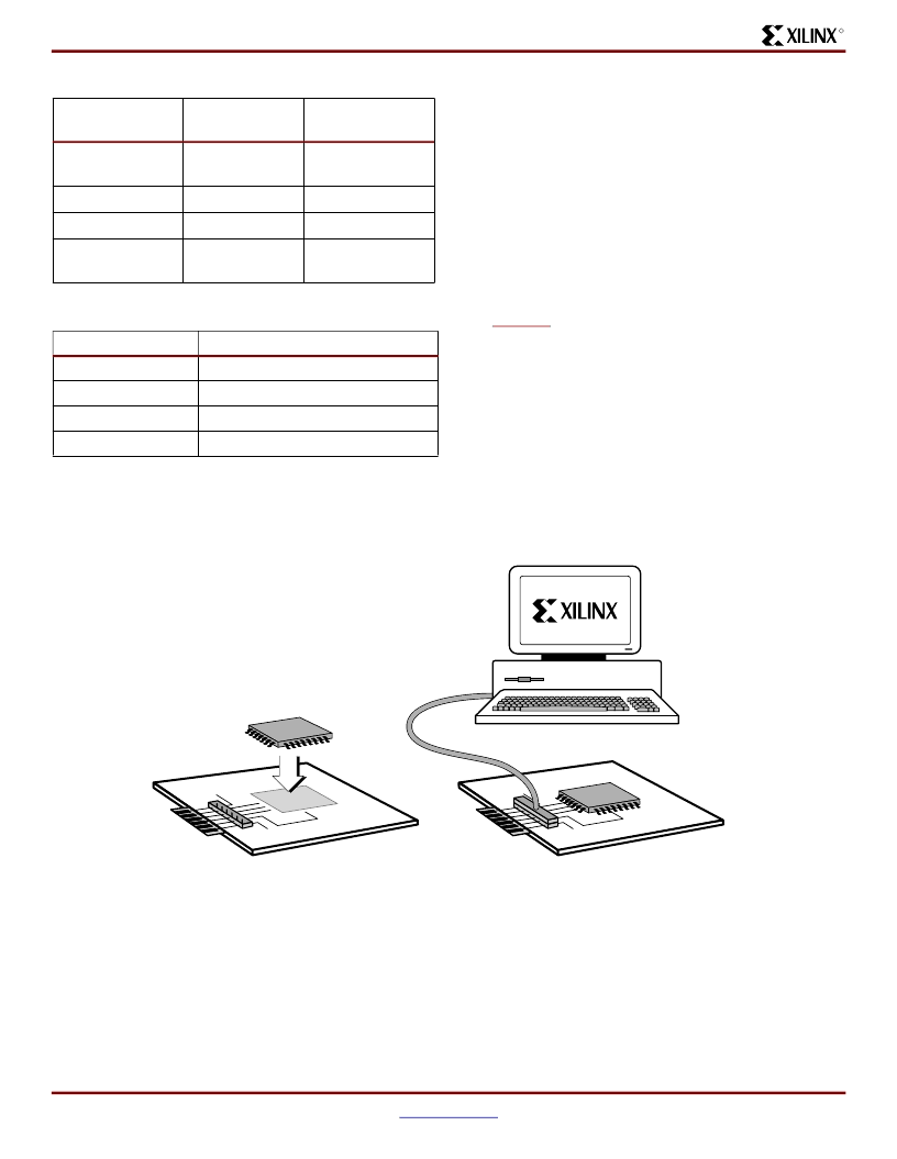
Figure 2:
In-System Programming Operation (a) Solder Device to PCB and (b) Program Using Download Cable
DS026_02_06/1103
GND
V
CCINT
(a)
(b)
相關(guān)PDF資料 |
PDF描述 |
|---|---|
| XC18V04PC44C | In-System Programmable Configuration PROMs |
| XC18V04SO20C | In-System Programmable Configuration PROMs |
| XC18V04VQ44C | In-System Programmable Configuration PROMs |
| XC18V512PC20C | In-System Programmable Configuration PROMs |
| XC18V512SO20C | In-System Programmable Configuration PROMs |
相關(guān)代理商/技術(shù)參數(shù) |
參數(shù)描述 |
|---|---|
| XC18V04PC44 | 制造商:XILINX 制造商全稱(chēng):XILINX 功能描述:In-System Programmable Configuration PROMs |
| XC18V04PC44C | 功能描述:IC PROM SER C-TEMP 3.3V 44-PLCC RoHS:否 類(lèi)別:集成電路 (IC) >> 存儲(chǔ)器 - 用于 FPGA 的配置 Proms 系列:- 產(chǎn)品變化通告:Product Discontinuation 28/Jul/2010 標(biāo)準(zhǔn)包裝:98 系列:- 可編程類(lèi)型:OTP 存儲(chǔ)容量:300kb 電源電壓:3 V ~ 3.6 V 工作溫度:-40°C ~ 85°C 封裝/外殼:8-SOIC(0.154",3.90mm 寬) 供應(yīng)商設(shè)備封裝:8-TSOP 包裝:管件 |
| XC18V04-PC44C | 制造商:Xilinx 功能描述: |
| XC18V04PC44C0100 | 制造商:Xilinx 功能描述: |
| XC18V04PC44C0901 | 制造商:Xilinx 功能描述: |
發(fā)布緊急采購(gòu),3分鐘左右您將得到回復(fù)。