- 您現(xiàn)在的位置:買賣IC網(wǎng) > PDF目錄374967 > XC18V04PC20C (Xilinx, Inc.) In-System Programmable Configuration PROMs PDF資料下載
參數(shù)資料
| 型號: | XC18V04PC20C |
| 廠商: | Xilinx, Inc. |
| 英文描述: | In-System Programmable Configuration PROMs |
| 中文描述: | 在系統(tǒng)可編程配置PROM的 |
| 文件頁數(shù): | 3/21頁 |
| 文件大?。?/td> | 230K |
| 代理商: | XC18V04PC20C |
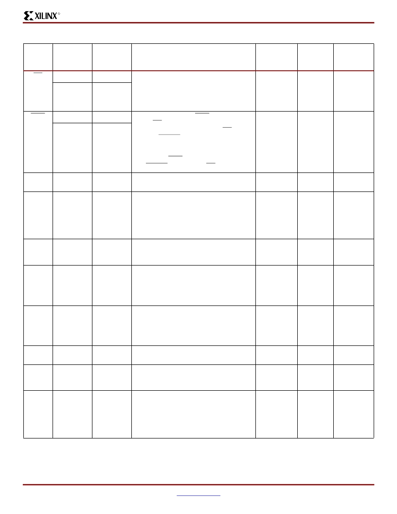
XC18V00 Series In-System Programmable Configuration PROMs
DS026 (v4.0) June 11, 2003
Product Specification
1-800-255-7778RCF
22
DATA OUT
Allows JTAG CONFIG instruction to
initiate FPGA configuration without
powering down FPGA. This is an
open-drain output that is pulsed Low by
the JTAG CONFIG command.
10
16
7
(1)
21
OUTPUT
ENABLE
CEO
12
DATA OUT
Chip Enable Output (CEO) is connected
to the CE input of the next PROM in the
chain. This output is Low when CE is Low
and OE/RESET input is High, AND the
internal address counter has been
incremented beyond its Terminal Count
(TC) value. CEO returns to High when
OE/RESET goes Low or CE goes High.
21
27
13
11
OUTPUT
ENABLE
GND
GND is the ground connection.
6, 18, 28 &
41
3, 12, 24
& 34
11
TMS
MODE
SELECT
The state of TMS on the rising edge of
TCK determines the state transitions at
the Test Access Port (TAP) controller.
TMS has an internal 50K ohm resistive
pull-up on it to provide a logic
“
1
”
to the
device if the pin is not driven.
5
11
5
TCK
CLOCK
This pin is the JTAG test clock. It
sequences the TAP controller and all the
JTAG test and programming electronics.
7
13
6
TDI
DATA IN
This pin is the serial input to all JTAG
instruction and data registers. TDI has an
internal 50K ohm resistive pull-up on it to
provide a logic
“
1
”
to the system if the pin
is not driven.
3
9
4
TDO
DATA OUT
This pin is the serial output for all JTAG
instruction and data registers. TDO has
an internal 50K ohm resistive pull-up on it
to provide a logic
“
1
”
to the system if the
pin is not driven.
31
37
17
V
CCINT
Positive 3.3V supply voltage for internal
logic.
17, 35 &
38
(3)
23, 41 &
44
(3)
18 & 20
(3)
V
CCO
Positive 3.3V or 2.5V supply voltage
connected to the input buffers
(2)
and
output voltage drivers.
8, 16, 26 &
36
14, 22, 32
& 42
19
NC
No connects.
1, 2, 4,
11, 12, 20,
22, 23, 24,
30, 32, 33,
34, 37, 39,
44
1, 6, 7, 8,
10, 17, 18,
26, 28, 29,
30, 36, 38,
39, 40, 43
Notes:
1.
By default, pin 7 is the D4 pin in the 20-pin packages. However, CF --> D4 programming option can be set to override the default and route
the CF function to pin 7 in the Serial mode.
For devices with IDCODES 0502x093h, the input buffers are supplied by V
.
For devices with IDCODES, 0503x093h, these V
pins are no connects: pin 38 in 44-pin VQFP package, pin 44 in 44-pin PLCC
package and pin 20 in 20-pin SOIC and20-pin PLCC packages.
2.
3.
Table 1:
Pin Names and Descriptions
(Continued)
Pin
Name
Boundary
Scan
Order
Function
Pin Description
44-pin
VQFP
44-pin
PLCC
20-pin
SOIC &
PLCC
相關(guān)PDF資料 |
PDF描述 |
|---|---|
| XC18V04PC44C | In-System Programmable Configuration PROMs |
| XC18V04SO20C | In-System Programmable Configuration PROMs |
| XC18V04VQ44C | In-System Programmable Configuration PROMs |
| XC18V512PC20C | In-System Programmable Configuration PROMs |
| XC18V512SO20C | In-System Programmable Configuration PROMs |
相關(guān)代理商/技術(shù)參數(shù) |
參數(shù)描述 |
|---|---|
| XC18V04PC44 | 制造商:XILINX 制造商全稱:XILINX 功能描述:In-System Programmable Configuration PROMs |
| XC18V04PC44C | 功能描述:IC PROM SER C-TEMP 3.3V 44-PLCC RoHS:否 類別:集成電路 (IC) >> 存儲器 - 用于 FPGA 的配置 Proms 系列:- 產(chǎn)品變化通告:Product Discontinuation 28/Jul/2010 標(biāo)準(zhǔn)包裝:98 系列:- 可編程類型:OTP 存儲容量:300kb 電源電壓:3 V ~ 3.6 V 工作溫度:-40°C ~ 85°C 封裝/外殼:8-SOIC(0.154",3.90mm 寬) 供應(yīng)商設(shè)備封裝:8-TSOP 包裝:管件 |
| XC18V04-PC44C | 制造商:Xilinx 功能描述: |
| XC18V04PC44C0100 | 制造商:Xilinx 功能描述: |
| XC18V04PC44C0901 | 制造商:Xilinx 功能描述: |
發(fā)布緊急采購,3分鐘左右您將得到回復(fù)。