- 您現(xiàn)在的位置:買賣IC網(wǎng) > PDF目錄372313 > ST901 (意法半導(dǎo)體) HIGH VOLTAGE IGNITION COIL DRIVER NPN POWER DARLINGTON PDF資料下載
參數(shù)資料
| 型號: | ST901 |
| 廠商: | 意法半導(dǎo)體 |
| 英文描述: | HIGH VOLTAGE IGNITION COIL DRIVER NPN POWER DARLINGTON |
| 中文描述: | 高壓點火線圈驅(qū)動達林頓NPN電源 |
| 文件頁數(shù): | 55/199頁 |
| 文件大小: | 2813K |
| 代理商: | ST901 |
第1頁第2頁第3頁第4頁第5頁第6頁第7頁第8頁第9頁第10頁第11頁第12頁第13頁第14頁第15頁第16頁第17頁第18頁第19頁第20頁第21頁第22頁第23頁第24頁第25頁第26頁第27頁第28頁第29頁第30頁第31頁第32頁第33頁第34頁第35頁第36頁第37頁第38頁第39頁第40頁第41頁第42頁第43頁第44頁第45頁第46頁第47頁第48頁第49頁第50頁第51頁第52頁第53頁第54頁當前第55頁第56頁第57頁第58頁第59頁第60頁第61頁第62頁第63頁第64頁第65頁第66頁第67頁第68頁第69頁第70頁第71頁第72頁第73頁第74頁第75頁第76頁第77頁第78頁第79頁第80頁第81頁第82頁第83頁第84頁第85頁第86頁第87頁第88頁第89頁第90頁第91頁第92頁第93頁第94頁第95頁第96頁第97頁第98頁第99頁第100頁第101頁第102頁第103頁第104頁第105頁第106頁第107頁第108頁第109頁第110頁第111頁第112頁第113頁第114頁第115頁第116頁第117頁第118頁第119頁第120頁第121頁第122頁第123頁第124頁第125頁第126頁第127頁第128頁第129頁第130頁第131頁第132頁第133頁第134頁第135頁第136頁第137頁第138頁第139頁第140頁第141頁第142頁第143頁第144頁第145頁第146頁第147頁第148頁第149頁第150頁第151頁第152頁第153頁第154頁第155頁第156頁第157頁第158頁第159頁第160頁第161頁第162頁第163頁第164頁第165頁第166頁第167頁第168頁第169頁第170頁第171頁第172頁第173頁第174頁第175頁第176頁第177頁第178頁第179頁第180頁第181頁第182頁第183頁第184頁第185頁第186頁第187頁第188頁第189頁第190頁第191頁第192頁第193頁第194頁第195頁第196頁第197頁第198頁第199頁
55/199
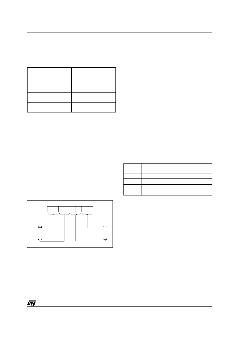
ST90158 - INTERRUPTS
4.6 EXTERNAL INTERRUPTS
The standard ST9 core contains 8 external inter-
rupts sources grouped into four pairs.
Table 10. External Interrupt Channel Grouping
Each source has a trigger control bit TEA0,..TED1
(R242,EITR.0,..,7 Page 0) to select triggering on
the rising or falling edge of the external pin. If the
Trigger control bit is set to “1”, the corresponding
pending bit IPA0,..,IPD1 (R243,EIPR.0,..,7 Page
0) is set on the input pin rising edge, if it is cleared,
the pending bit is set on the falling edge of the in-
put pin. Each source can be individually masked
through
the
corresponding
IMA0,..,IMD1 (EIMR.7,..,0). See
Figure 26
.
The priority level of the external interrupt sources
can be programmed among the eight priority lev-
els with the control register EIPLR (R245). The pri-
ority level of each pair is software defined using
the bits PRL2, PRL1. For each pair, the even
channel (A0,B0,C0,D0) of the group has the even
priority level and the odd channel (A1,B1,C1,D1)
has the odd (lower) priority level.
control
bit
Figure 25. Priority Level Examples
n
Figure 25
shows an example of priority levels.
Figure 26
gives an overview of the External inter-
rupt control bits and vectors.
– The source of the interrupt channel A0 can be
selected between the external pin INT0 (when
IA0S = “1”, the reset value) or the On-chip Timer/
Watchdog peripheral (when IA0S = “0”).
– The source of the interrupt channel B0 can be
selected between the external pin INT2 (when
(SPEN,BMS)=(0,0)) or the on-chip SPI peripher-
al.
– The source of the interrupt channel C0 can be
selected between the external pin INT4 (when
INTS = “1”) or the on-chip Standard Timer.
– The source of the interrupt channel D0 can be
selected between the external pin INT6 (when
INT_SEL = “0”) or the on-chip RCCU.
Warning:
When using channels shared by both
external interrupts and peripherals, special care
must be taken to configure their control registers
for both peripherals and interrupts.
Table 11. Multiplexed Interrupt Sources
External Interrupt
INT7
INT6
INT5
INT4
INT3
INT2
INT1
INT0
Channel
INTD1
INTD0
INTC1
INTC0
INTB1
INTB0
INTA1
INTA0
1
0
0
1
0
0
1
PL2D PL1D PL2C PL1C PL2B PL1B PL2A PL1A
INT.D1:
INT.C1: 001=1
INT.D0:
SOURCE
PRIORITY
PRIORITY
SOURCE
INT.A0: 010=2
INT.A1: 011=3
INT.B1: 101=5
INT.B0: 100=4
INT.C0: 000=0
EIPLR
VR000151
0
100=4
101=5
Channel
Internal Interrupt
Source
Timer/Watchdog
SPI Interrupt
STIM Timer
RCCU
External Interrupt
Source
INT0
INT2
INT4
INT6
INTA0
INTB0
INTC0
INTD0
9
相關(guān)PDF資料 |
PDF描述 |
|---|---|
| ST901T | HIGH VOLTAGE IGNITION COIL DRIVER NPN POWER DARLINGTON |
| ST9291J7B1 | Microcontroller |
| ST9291N2B1 | Microcontroller |
| ST9291N3B1 | Microcontroller |
| ST9291N4B1 | Microcontroller |
相關(guān)代理商/技術(shù)參數(shù) |
參數(shù)描述 |
|---|---|
| ST9011 | 制造商:SEMTECH_ELEC 制造商全稱:SEMTECH ELECTRONICS LTD. 功能描述:NPN Silicon Epitaxial Planar Transistor |
| ST9012 | 制造商:SEMTECH_ELEC 制造商全稱:SEMTECH ELECTRONICS LTD. 功能描述:PNP Silicon Epitaxial Planar Transistor |
| ST90-125L2KI | 功能描述:CAP TANT 90UF 125V 10% AXIAL RoHS:否 類別:電容器 >> 鉭 系列:SuperTan® ST 標準包裝:1,000 系列:TANTAMOUNT® 695D 電容:3.3µF 電壓 - 額定:50V 容差:±20% ESR(等效串聯(lián)電阻):3.2 歐姆 類型:保形涂層 工作溫度:-55°C ~ 125°C 安裝類型:表面貼裝 封裝/外殼:2414(6034 公制) 尺寸/尺寸:0.236" L x 0.135" W(6.00mm x 3.43mm) 高度 - 座高(最大):0.085"(2.16mm) 引線間隔:- 制造商尺寸代碼:F 特點:通用 包裝:帶卷 (TR) 壽命@溫度:- |
| ST9013 | 制造商:SEMTECH_ELEC 制造商全稱:SEMTECH ELECTRONICS LTD. 功能描述:NPN Silicon Epitaxial Planar Transistor |
| ST90135 | 制造商:STMICROELECTRONICS 制造商全稱:STMicroelectronics 功能描述:8/16-BIT MCU FAMILY WITH UP TO 64K ROM/OTP/EPROM AND UP TO 2K RAM |
發(fā)布緊急采購,3分鐘左右您將得到回復(fù)。