- 您現(xiàn)在的位置:買賣IC網(wǎng) > PDF目錄372313 > ST90158M7T6 8-BIT MICROCONTROLLER PDF資料下載
參數(shù)資料
| 型號: | ST90158M7T6 |
| 元件分類: | 8位微控制器 |
| 英文描述: | 8-BIT MICROCONTROLLER |
| 中文描述: | 8位微控制器 |
| 文件頁數(shù): | 154/199頁 |
| 文件大小: | 2813K |
| 代理商: | ST90158M7T6 |
第1頁第2頁第3頁第4頁第5頁第6頁第7頁第8頁第9頁第10頁第11頁第12頁第13頁第14頁第15頁第16頁第17頁第18頁第19頁第20頁第21頁第22頁第23頁第24頁第25頁第26頁第27頁第28頁第29頁第30頁第31頁第32頁第33頁第34頁第35頁第36頁第37頁第38頁第39頁第40頁第41頁第42頁第43頁第44頁第45頁第46頁第47頁第48頁第49頁第50頁第51頁第52頁第53頁第54頁第55頁第56頁第57頁第58頁第59頁第60頁第61頁第62頁第63頁第64頁第65頁第66頁第67頁第68頁第69頁第70頁第71頁第72頁第73頁第74頁第75頁第76頁第77頁第78頁第79頁第80頁第81頁第82頁第83頁第84頁第85頁第86頁第87頁第88頁第89頁第90頁第91頁第92頁第93頁第94頁第95頁第96頁第97頁第98頁第99頁第100頁第101頁第102頁第103頁第104頁第105頁第106頁第107頁第108頁第109頁第110頁第111頁第112頁第113頁第114頁第115頁第116頁第117頁第118頁第119頁第120頁第121頁第122頁第123頁第124頁第125頁第126頁第127頁第128頁第129頁第130頁第131頁第132頁第133頁第134頁第135頁第136頁第137頁第138頁第139頁第140頁第141頁第142頁第143頁第144頁第145頁第146頁第147頁第148頁第149頁第150頁第151頁第152頁第153頁當(dāng)前第154頁第155頁第156頁第157頁第158頁第159頁第160頁第161頁第162頁第163頁第164頁第165頁第166頁第167頁第168頁第169頁第170頁第171頁第172頁第173頁第174頁第175頁第176頁第177頁第178頁第179頁第180頁第181頁第182頁第183頁第184頁第185頁第186頁第187頁第188頁第189頁第190頁第191頁第192頁第193頁第194頁第195頁第196頁第197頁第198頁第199頁
154/199
ST90158 - MULTIPROTOCOL SERIAL COMMUNICATIONS INTERFACE (SCI-M)
MULTIPROTOCOL SERIAL COMMUNICATIONS INTERFACE
(Cont’d)
9.6.8 Input Signals
SIN: Serial Data Input
. This pin is the serial data
input to the SCI receiver shift register.
TXCLK: External Transmitter Clock Input
. This
pin is the external input clock driving the SCI trans-
mitter. The TXCLK frequency must be greater than
or equal to 16 times the transmitter data rate (de-
pending whether the X16 or the X1 clock have
been selected). A 50% duty cycle is required for
this input and must have a period of at least twice
INTCLK. The use of the TXCLK pin is optional.
RXCLK: External Receiver Clock Input.
This in-
put is the clock to the SCI receiver when using an
external clock source connected to the baud rate
generator. INTCLK is normally the clock source. A
50% duty cycle is required for this input and must
have a period of at least twice INTCLK. Use of RX-
CLK is optional.
DCD: Data Carrier Detect.
This input is enabled
only in Synchronous mode; it works as a gate for
the RXCLK clock and informs the MCU that an
emitting device is transmitting a synchronous
frame. The active level can be programmed as 1
or 0 and must be provided at least one INTCLK pe-
riod before the first active edge of the input clock.
9.6.9 Output Signals
SOUT: Serial Data Output.
This Alternate Func-
tion output signal is the serial data output for the
SCI transmitter in all operating modes.
CLKOUT: Clock Output
. The alternate Function
of this pin outputs either the data clock from the
transmitter in Serial Expansion or Synchronous
modes, or the clock output from the Baud Rate
Generator. In Serial expansion mode it will clock
only the data portion of the frame and its stand-by
state is high: data is valid on the rising edge of the
clock. Even in Synchronous mode CLKOUT will
only clock the data portion of the frame, but the
stand-by level and active edge polarity are pro-
grammable by the user.
When Synchronous mode is disabled (SMEN in
SICR is reset), the state of the XTCLK and OCLK
bits in CCR determine the source of CLKOUT; '11'
enables the Serial Expansion Mode.
When the Synchronous mode is enabled (SMEN
in SICR is set), the state of the XTCLK and OCLK
bits in CCR determine the source of CLKOUT; '00'
disables it for PLM applications.
RTS: Request To Send.
This output Alternate
Function is only enabled in Synchronous mode; it
becomes active when the Least Significant Bit of
the data frame is sent to the Serial Output Pin
(SOUT) and indicates to the target device that the
MCU is about to send a synchronous frame; it re-
turns to its stand-by value just after the last active
edge of CLKOUT (MSB transmitted). The active
level can be programmed high or low.
SDS: Synchronous Data Strobe.
This output Al-
ternate function is only enabled in Synchronous
mode; it becomes active high when the Least Sig-
nificant Bit is sent to the Serial Output Pins
(SOUT) and indicates to the target device that the
MCU is about to send the first bit for each synchro-
nous frame. It is active high on the first bit and it is
low for all the rest of the frame. The active level
can not be programmed.
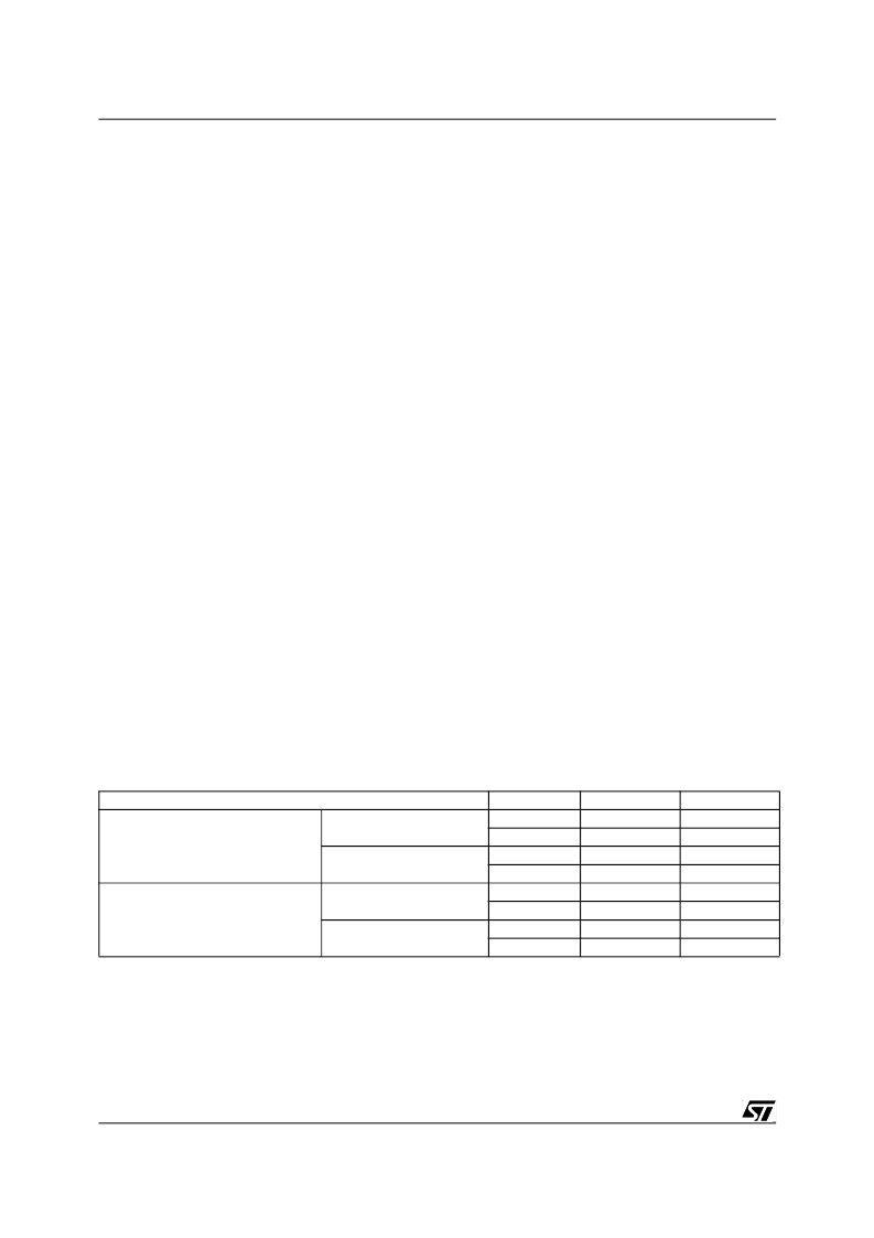
Figure 85. Receiver and Transmitter Clock Frequencies
Note:
The internal receiver and transmitter clocks
are the ones applied to the Tx and Rx shift regis-
ters (see
Figure 76
).
Min
0
0
0
0
0
0
0
0
Max
Conditions
1x mode
16x mode
1x mode
16x mode
1x mode
16x mode
1x mode
16x mode
Receiver Clock Frequency
External RXCLK
INTCLK/8
INTCLK/4
INTCLK/8
INTCLK/2
INTCLK/8
INTCLK/4
INTCLK/8
INTCLK/2
Internal Receiver Clock
Transmitter Clock Frequency
External TXCLK
Internal Transmitter Clock
9
相關(guān)PDF資料 |
PDF描述 |
|---|---|
| ST90158M9 | 8/16-BIT MICROCONTROLLER (MCU) WITH 16 TO 64K ROM. OTP OR EPROM. 512 TO 2K RAM - ST9 + FAMILY |
| ST90158M9LVT6 | 8/16-BIT MICROCONTROLLER (MCU) WITH 16 TO 64K ROM. OTP OR EPROM. 512 TO 2K RAM - ST9 + FAMILY |
| ST90158M9T6 | 8-BIT MICROCONTROLLER |
| ST90R158M9LVT6 | FUSE,5A,250V,5X20MM,FAST ACTING |
| ST90R158T6 | 8/16-BIT MICROCONTROLLER (MCU) WITH 16 TO 64K ROM. OTP OR EPROM. 512 TO 2K RAM - ST9 + FAMILY |
相關(guān)代理商/技術(shù)參數(shù) |
參數(shù)描述 |
|---|---|
| ST90158M9 | 制造商:未知廠家 制造商全稱:未知廠家 功能描述:8/16-BIT MICROCONTROLLER (MCU) WITH 16 TO 64K ROM. OTP OR EPROM. 512 TO 2K RAM - ST9 + FAMILY |
| ST90158M9LVT6 | 制造商:未知廠家 制造商全稱:未知廠家 功能描述:8/16-BIT MICROCONTROLLER (MCU) WITH 16 TO 64K ROM. OTP OR EPROM. 512 TO 2K RAM - ST9 + FAMILY |
| ST90158M9Q6 | 制造商:STMICROELECTRONICS 制造商全稱:STMicroelectronics 功能描述:8/16-BIT MCU FAMILY WITH UP TO 64K ROM/OTP/EPROM AND UP TO 2K RAM |
| ST90158M9T1 | 制造商:STMICROELECTRONICS 制造商全稱:STMicroelectronics 功能描述:8/16-BIT MCU FAMILY WITH UP TO 64K ROM/OTP/EPROM AND UP TO 2K RAM |
| ST90158M9T6 | 制造商:未知廠家 制造商全稱:未知廠家 功能描述:8-Bit Microcontroller |
發(fā)布緊急采購,3分鐘左右您將得到回復(fù)。