- 您現(xiàn)在的位置:買賣IC網(wǎng) > PDF目錄372303 > ST52F514F1M6 IC MAX 7000 CPLD 256 208-PQFP PDF資料下載
參數(shù)資料
| 型號(hào): | ST52F514F1M6 |
| 英文描述: | IC MAX 7000 CPLD 256 208-PQFP |
| 中文描述: | 微控制器 |
| 文件頁(yè)數(shù): | 66/106頁(yè) |
| 文件大?。?/td> | 648K |
| 代理商: | ST52F514F1M6 |
第1頁(yè)第2頁(yè)第3頁(yè)第4頁(yè)第5頁(yè)第6頁(yè)第7頁(yè)第8頁(yè)第9頁(yè)第10頁(yè)第11頁(yè)第12頁(yè)第13頁(yè)第14頁(yè)第15頁(yè)第16頁(yè)第17頁(yè)第18頁(yè)第19頁(yè)第20頁(yè)第21頁(yè)第22頁(yè)第23頁(yè)第24頁(yè)第25頁(yè)第26頁(yè)第27頁(yè)第28頁(yè)第29頁(yè)第30頁(yè)第31頁(yè)第32頁(yè)第33頁(yè)第34頁(yè)第35頁(yè)第36頁(yè)第37頁(yè)第38頁(yè)第39頁(yè)第40頁(yè)第41頁(yè)第42頁(yè)第43頁(yè)第44頁(yè)第45頁(yè)第46頁(yè)第47頁(yè)第48頁(yè)第49頁(yè)第50頁(yè)第51頁(yè)第52頁(yè)第53頁(yè)第54頁(yè)第55頁(yè)第56頁(yè)第57頁(yè)第58頁(yè)第59頁(yè)第60頁(yè)第61頁(yè)第62頁(yè)第63頁(yè)第64頁(yè)第65頁(yè)當(dāng)前第66頁(yè)第67頁(yè)第68頁(yè)第69頁(yè)第70頁(yè)第71頁(yè)第72頁(yè)第73頁(yè)第74頁(yè)第75頁(yè)第76頁(yè)第77頁(yè)第78頁(yè)第79頁(yè)第80頁(yè)第81頁(yè)第82頁(yè)第83頁(yè)第84頁(yè)第85頁(yè)第86頁(yè)第87頁(yè)第88頁(yè)第89頁(yè)第90頁(yè)第91頁(yè)第92頁(yè)第93頁(yè)第94頁(yè)第95頁(yè)第96頁(yè)第97頁(yè)第98頁(yè)第99頁(yè)第100頁(yè)第101頁(yè)第102頁(yè)第103頁(yè)第104頁(yè)第105頁(yè)第106頁(yè)
ST52F510/F513/F514
66/106
The conversion continues until a stop command is
executed by writing a ‘0’ in the apposite AD_CR
Configuration Register bit STR.
10.3.4
In this mode (CONT=1, SEQ=1) a continuous
conversion flow is entered by a start event on the
selected channel sequence. The CH2-0 bits
indicate the last channel of the sequence.
At the end of each conversion the relative Input
Registers are updated with the last conversion
results, while the former values are lost.
The conversion continues until a stop command is
executed by writing a ‘0’ in the apposite AD_CR
Configuration Register bit STR.
Multiple Channels Continuous Mode.
10.4 Power Down Mode
Before enabling any A/D operation modes, set the
Power On bit (POW) of the Configuration Register
AD_CR to ‘1’ and then start the A/D Converter by
setting the STR bit. It is suggested to execute the
pre-charging after the Power on to speed-up the
auto calibrationprocess. Clearing the Power Onbit
is useful when the A/D is not used, reducing the
total chippower consumption. This state is also the
reset configuration and it is forced by hardware
when the core is in HALT state (after a HALT
instruction execution).
10.5 A/D Converter Register Description
The following registers are related to the use of the
A/D Converter.
10.5.1 A/D Converter Configuration Registers.
A/D Converter Control Register 1 (AD_CR1)
Configuration Register 8 (08h) Read/Write
Reset Value: 0000 0000 (00h)
Bit 7-5:
CH2-CH0
Channel Number
The number specified identifies the number
of channels to be converted (Multiple
Channel mode) or the channel to be
converted (One Channel mode)
Bit 4:
SCK
A/D speed mode
0: Slow mode (800 kHz)
1: Fast mode (1600 kHz)
Bit 3:
SEQ
One/Multiple Channel Mode
0: One Channel Mode
1: Multiple Channel Mode
Bit 2:
POW
A/D Converter Power Down/Up
0: Power down
1: Power up
Bit 1:
CONT
Single/Continuous Mode
0: Single Mode
1: Continuous Mode
Bit 0:
STR
A/D Converter Start bit
0: A/D Converter stopped
1: A/D Converter started
A/D Converter Control Register 2 (AD_CR2)
Configuration Register 47 (02Fh) Read/Write
Reset Value: 0000 0000 (00h)
Bit 7-5: not used
Bit 4:
PRECH
Pre-charging process on/off
0: Pre-charge on (default)
1: Pre-charge off
Bit 3:
REF
Voltage Reference (VREF) source
0: Internal from Vdd
1: External from VREF pin
Bit 2:
RESOL
8/10 bits resolution
0: 10 bits
1: 8 bits
Bit 1:
INT1
Overflow interrupt mask
0: interrupt disabled
1: interrupt enabled (if MSKAD=1)
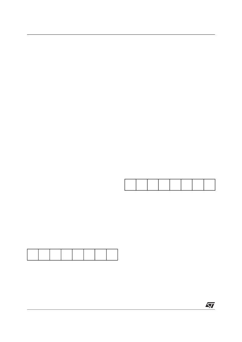
7
0
CH2
CH1
CH0
SCK
SEQ
POW
CONT
STR
7
0
-
-
-
PRECH
REF
RESOL
INT1
INT0
相關(guān)PDF資料 |
PDF描述 |
|---|---|
| ST52F514F3B6 | IC MAX 7000 CPLD 256 208-PQFP |
| ST52F514F3M6 | IC MAX 7000 CPLD 256 256-FBGA |
| ST52F514G0B6 | IC MAX 7000 CPLD 256 256-FBGA |
| ST52F514G0M6 | IC MAX 7000 CPLD 64 100-TQFP |
| ST52F514G1B6 | IC MAX 7000 CPLD 64 100-TQFP |
相關(guān)代理商/技術(shù)參數(shù) |
參數(shù)描述 |
|---|---|
| ST52F514F3B6 | 制造商:未知廠家 制造商全稱:未知廠家 功能描述:Microcontroller |
| ST52F514F3M6 | 制造商:未知廠家 制造商全稱:未知廠家 功能描述:Microcontroller |
| ST52F514FMB6 | 制造商:STMICROELECTRONICS 制造商全稱:STMicroelectronics 功能描述:8-BIT INTELLIGENT CONTROLLER UNIT ICU Two Timer/PWMs, ADC, I2C, SPI, SCI |
| ST52F514FMM6 | 制造商:STMICROELECTRONICS 制造商全稱:STMicroelectronics 功能描述:8-BIT INTELLIGENT CONTROLLER UNIT ICU Two Timer/PWMs, ADC, I2C, SPI, SCI |
| ST52F514G0B6 | 制造商:未知廠家 制造商全稱:未知廠家 功能描述:Microcontroller |
發(fā)布緊急采購(gòu),3分鐘左右您將得到回復(fù)。