- 您現(xiàn)在的位置:買賣IC網(wǎng) > PDF目錄374932 > SSM5G02TU (Toshiba Corporation) DC-DC Converter PDF資料下載
參數(shù)資料
| 型號(hào): | SSM5G02TU |
| 廠商: | Toshiba Corporation |
| 元件分類: | DC/DC變換器 |
| 英文描述: | DC-DC Converter |
| 中文描述: | DC - DC轉(zhuǎn)換 |
| 文件頁(yè)數(shù): | 1/10頁(yè) |
| 文件大?。?/td> | 197K |
| 代理商: | SSM5G02TU |
SSM5G02TU
2007-11-01
1
Silicon P Channel MOS Type (U-MOS
II
)/Silicon Epitaxial Schottky Barrier Diode
SSM5G02TU
DC-DC Converter
Combined Pch MOSFET and Schottky Diode into one Package.
Low R
DS (ON)
and Low V
F
Absolute Maximum Ratings
(Ta
=
25°C) MOSFET
Characteristics
Symbol
Rating
Unit
Drain-Source voltage
V
DS
12
V
Gate-Source voltage
V
GSS
±
12
V
DC
I
D
1.0
Drain current
Pulse
I
DP
(Note 2)
2.0
A
P
D
(Note 1)
0.5
Drain power dissipation
t
=
10s
0.8
W
Channel temperature
T
ch
150
°
C
Absolute Maximum Ratings
(Ta
=
25°C) SCHOTTKY
DIODE
Characteristics
Symbol
Rating
Unit
Maximum (peak) reverse voltage
V
RM
15
V
Reverse voltage
V
R
12
V
Average forward current
I
O
0.5
A
Peak one cycle surge forward current
(non-repetitive)
I
FSM
2 (50 Hz)
A
Junction temperature
T
j
125
°
C
Absolute Maximum Ratings
(Ta
=
25°C) MOSFET, DIODE COMMON
Characteristics
Symbol
Rating
Unit
Storage temperature
T
stg
55~125
°
C
Operating temperature
T
opr
(Note 3)
40~85
°
C
Note:
Using continuously under heavy loads (e.g. the application of high temperature/current/voltage and the
significant change in temperature, etc.) may cause this product to decrease in the reliability significantly
even if the operating conditions (i.e. operating temperature/current/voltage, etc.) are within the absolute
maximum ratings.
Please design the appropriate reliability upon reviewing the Toshiba Semiconductor Reliability Handbook
(“Handling Precautions”/“Derating Concept and Methods”) and individual reliability data (i.e. reliability test
report and estimated failure rate, etc).
Note 1: Mounted on FR4 board
(25.4 mm
×
25.4 mm
×
1.6 t, Cu pad: 645 mm
2
)
Note 2: The pulse width limited by max channel temperature.
Note 3: Operating temperature limited by max channel temperature and max junction temperature.
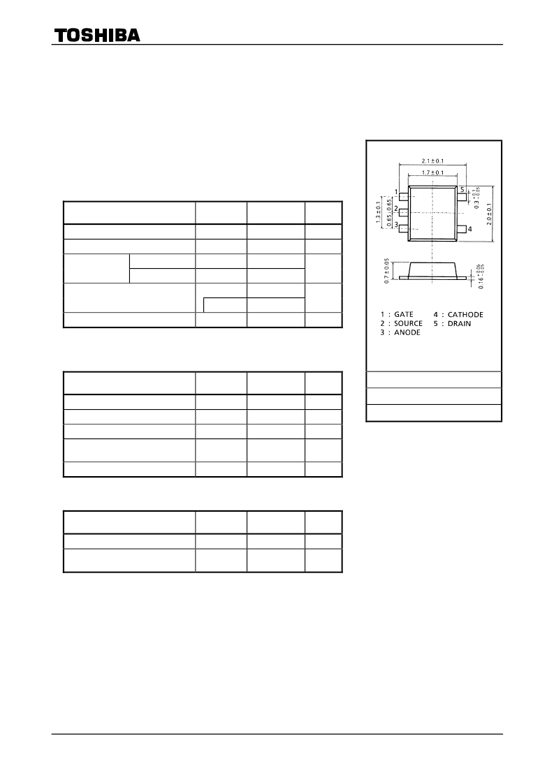
Unit: mm
UFV
JEDEC
JEITA
TOSHIBA
2-2R1A
Weight: 7 mg (typ.)
相關(guān)PDF資料 |
PDF描述 |
|---|---|
| SSM5G04TU | DC-DC Converter |
| SSM5G09TU | DC-DC Converter |
| SSM5H01TU | DC-DC Converter |
| SSM5H03TU | DC-DC Converter |
| SSM5H05TU | DC-DC Converter |
相關(guān)代理商/技術(shù)參數(shù) |
參數(shù)描述 |
|---|---|
| SSM5G04TU | 制造商:TOSHIBA 制造商全稱:Toshiba Semiconductor 功能描述:DC-DC Converter |
| SSM5G09TU | 制造商:TOSHIBA 制造商全稱:Toshiba Semiconductor 功能描述:DC-DC Converter |
| SSM5G10TU | 制造商:TOSHIBA 制造商全稱:Toshiba Semiconductor 功能描述:DC-DC Converter Applications |
| SSM5G10TU(TE85L,F) | 制造商:Toshiba America Electronic Components 功能描述:MOSFET P-CH 20V 1.5A UFV - Tape and Reel |
| SSM5G11TU | 制造商:TOSHIBA 制造商全稱:Toshiba Semiconductor 功能描述:DC-DC Converter Applications |
發(fā)布緊急采購(gòu),3分鐘左右您將得到回復(fù)。