- 您現(xiàn)在的位置:買賣IC網(wǎng) > PDF目錄374928 > SSD1812Z (Electronic Theatre Controls, Inc.) LCD Segment / Common Driver with Controller CMOS PDF資料下載
參數(shù)資料
| 型號: | SSD1812Z |
| 廠商: | Electronic Theatre Controls, Inc. |
| 英文描述: | LCD Segment / Common Driver with Controller CMOS |
| 中文描述: | LCD段/與普通的CMOS驅(qū)動器控制器 |
| 文件頁數(shù): | 9/28頁 |
| 文件大小: | 434K |
| 代理商: | SSD1812Z |
第1頁第2頁第3頁第4頁第5頁第6頁第7頁第8頁當(dāng)前第9頁第10頁第11頁第12頁第13頁第14頁第15頁第16頁第17頁第18頁第19頁第20頁第21頁第22頁第23頁第24頁第25頁第26頁第27頁第28頁
S OLOMON
SSD1812
9
REV 1.2
12/99
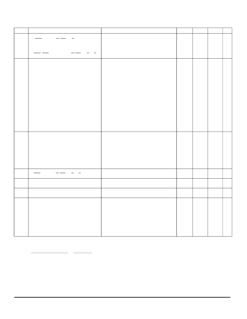
ELECTRICAL CHARACTERISTICS
(Voltage Referenced to V
SS
, V
DD
=1.8 to 3.5V, T
A
=25°C; unless otherwise specified.)
* The formula for the temperature coefficient is:
Symbol
Parameter
Test Condition
Min
Typ
Max
Unit
V
IH1
V
IL1
Input high voltage
(RES, D
0
-D
7
,R/W(WR), D/C)
Input Low voltage
(RES, CS1,CS2, D
0
-D
7
, R/W(WR), D/C, S/P)
LCD Display Voltage Output
(V
L2
, V
L3
, V
L4
, V
L5
, V
L6
Pins)
0.8*V
DD
0
-
-
V
DD
0.2*V
DD
V
V
V
L2
V
L3
V
L4
V
L5
V
L6
V
L2
V
L3
V
L4
V
L5
V
L6
V
L2
V
L3
V
L4
V
L5
V
L6
I
OH
LCD Display Voltage Output
(V
L2
, V
L3
, V
L4
, V
L5
, V
L6
Pins)
LCD Display Voltage Input
(V
L2
, V
L3
,V
L4
, V
L5
, V
L6
Pins)
Voltage reference to V
DD
, Smart Bias Divider
Enabled, 1:6 bias ratio
Voltage reference to V
DD
, Smart Bias Divider
Enabled, 1:8 bias ratio
Voltage reference to V
DD
, External Voltage Gener-
ator, Smart Bias Divider Disabled
-
-
-
-
-
-
-
-
-
-
V
L3
V
L4
V
L5
V
L6
-12V
1/6*V
L6
2/6*V
L6
4/6*V
L6
5/6*V
L6
V
L6
1/8*V
L6
2/8*V
L6
6/8*V
L6
7/8*V
L6
V
L6
-
-
-
-
-
-
-
-
-
-
-
-
-
-
-
V
DD
V
L2
V
L3
V
L4
V
L5
-
V
V
V
V
V
V
V
V
V
V
V
V
V
V
V
I
OL
I
OZ
Output High Current Source
(D
0
-D
7
)
Output Low Current Drain
(D
0
-D
7
)
Output Tri-state Current Drain Source
(D
0
-D
7
)
Input Current
(RES, D
0
-D
7
, R/W(WR), D/C, S/P)
Input Capacitance
(all logic pins)
V
out
=V
DD
-0.4V
V
out
=0.4V
50
-
-1
-
-
-
-50
1
μ
A
μ
A
μ
A
I
IL
/I
IH
-1
-
1
μ
A
C
IN
-
5
7.5
pF
V
L6
Variation of V
L6
Output (V
DD
is fixed)
Regulator Enabled, Internal Contrast Control
Enabled, Set Contrast Control Register = 0
-
±
3
-
%
PTC0
PTC1
PTC2
PTC3
PTC4
PTC5
PTC6
PTC7
Temperature Coefficient Compensation
Flat Temperature Coefficient [POR]
Temperature Coefficient 1*
Temperature Coefficient 2*
Temperature Coefficient 3*
Temperature Coefficient 4*
Temperature Coefficient 5*
Temperature Coefficient 6*
Temperature Coefficient 7*
Voltage Regulator Enabled
Voltage Regulator Enabled
Voltage Regulator Enabled
Voltage Regulator Enabled
Voltage Regulator Enabled
Voltage Regulator Enabled
Voltage Regulator Enabled
Voltage Regulator Enabled
0
-0.075
-0.15
-0.20
-0.01
TBD
-0.10
TBD
-0.18
TBD
TBD
-0.25
-0.075
-0.15
-0.20
%/C
%/C
%/C
%/C
%/C
%/C
%/C
%/C
TC(%)=
V
ref
at 50°C - V
ref
at 0°C
50°C - 0°C
X
1
V
ref
at 25°CX100%
相關(guān)PDF資料 |
PDF描述 |
|---|---|
| SSD1815 | SEMICONDUCTOR TECHNICAL DATA |
| SSD1815T1R | SEMICONDUCTOR TECHNICAL DATA |
| SSD1815T2R | SEMICONDUCTOR TECHNICAL DATA |
| SSD1815T3R | SEMICONDUCTOR TECHNICAL DATA |
| SSD1815TR | SEMICONDUCTOR TECHNICAL DATA |
相關(guān)代理商/技術(shù)參數(shù) |
參數(shù)描述 |
|---|---|
| SSD1815 | 制造商:未知廠家 制造商全稱:未知廠家 功能描述:SEMICONDUCTOR TECHNICAL DATA |
| SSD1815B | 制造商:未知廠家 制造商全稱:未知廠家 功能描述:LCD Segment / Common Driver with Controller |
| SSD1815BT | 制造商:未知廠家 制造商全稱:未知廠家 功能描述:LCD Segment / Common Driver with Controller |
| SSD1815BT2 | 制造商:未知廠家 制造商全稱:未知廠家 功能描述:LCD Segment / Common Driver with Controller |
| SSD1815BZ | 制造商:未知廠家 制造商全稱:未知廠家 功能描述:LCD Segment / Common Driver with Controller |
發(fā)布緊急采購,3分鐘左右您將得到回復(fù)。