- 您現(xiàn)在的位置:買賣IC網(wǎng) > PDF目錄374927 > SSCP485 (Electronic Theatre Controls, Inc.) SSC P485 PL Transceiver IC PDF資料下載
參數(shù)資料
| 型號: | SSCP485 |
| 廠商: | Electronic Theatre Controls, Inc. |
| 英文描述: | SSC P485 PL Transceiver IC |
| 中文描述: | 南南合作P485特等收發(fā)芯片 |
| 文件頁數(shù): | 7/19頁 |
| 文件大?。?/td> | 109K |
| 代理商: | SSCP485 |
SSC P485 PL Transceiver IC
July 1998
7
Revision 5
24000828
ADVANCE INFORMATION
SSC P485 Power Line Interface
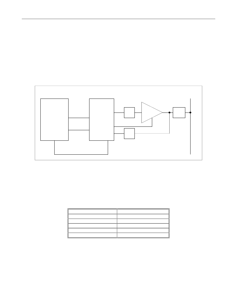
Analog data is transferred between the communication medium and the SSC P485 over the Signal In (SI) and
Signal Out (SO) pins (refer to Figure 5
). When transmitting, SSC “chirps” from the SSC P485 SO pin are filtered
by the output filter to remove harmonic energy (distortion) from the transmit signal and then amplified by the SSC
P111 Power Line Media Interface IC. The SSC P111 is a high-efficiency amplifier and tri-state switch specifically
designed for use in power line network systems. The amplifier is powered down and its output set to a high
impedance condition when the SSC P485 TS* signal is logic low, isolating the amplifier from the receive circuitry
and reducing node power consumption during receive operation. When the SSC P485 TS* signal is logic high,
the communication signal is routed to the communication medium through the coupling circuit (capacitor or
transformer). When receiving, the communication signal passes through the coupling circuit and is filtered by the
bandpass input filter. The resulting signal is then applied to the SSC P485 SI pin for processing. Refer to the
application reference shown in Figure 14.
Host micro with
internal UART
ILD
RXD
TXD
P485
IC
P111
IC
SO
TS*
SI
ILD
DI
RO
Single
Wire
input
filter
output
filter
medium
coupler
Figure 5. SSC P485 Medium Coupling
SSC P485 Message Format
The P485 requires the following message formatting:
Start bits
Data bits
Stop bits
Character gap
Message gap
Message length
1, logic low
8 or 9 (default 8)
1, logic high
0-4 bit times
12 bit times minimum
1 character minimum
相關(guān)PDF資料 |
PDF描述 |
|---|---|
| SSCP485PL | SSC P485 PL Transceiver IC |
| SSD-D50100CDM | LED DOT MATRIX |
| SSD-D64128CDM | 16Dot*32Dot LED DOT MATRIX |
| SSD-D6464SLMH-GREEN | LED DOT MATRIX |
| SSD-D6464SLMH-RED | LED DOT MATRIX |
相關(guān)代理商/技術(shù)參數(shù) |
參數(shù)描述 |
|---|---|
| SSCP485PL | 制造商:未知廠家 制造商全稱:未知廠家 功能描述:SSC P485 PL Transceiver IC |
| SSC-PHBMGSRT722 | 制造商:SEOUL 制造商全稱:Seoul Semiconductor 功能描述:TOP LED DEVICE |
| SSC-PNE87125181 | 制造商:Seiko Instruments Inc (SII) 功能描述: |
| SSC-PTR202 | 制造商:SEOUL 制造商全稱:Seoul Semiconductor 功能描述:Photo Transistor |
| SSC-PTR202-IX0 | 制造商:SEOUL 制造商全稱:Seoul Semiconductor 功能描述:Photo Transistor |
發(fā)布緊急采購,3分鐘左右您將得到回復(fù)。