- 您現(xiàn)在的位置:買賣IC網(wǎng) > PDF目錄374866 > SN74GTLPH16945VR (Texas Instruments, Inc.) 16-BIT LVTTL-TO-GTLP BUS TRANSCEIVER PDF資料下載
參數(shù)資料
| 型號: | SN74GTLPH16945VR |
| 廠商: | Texas Instruments, Inc. |
| 英文描述: | 16-BIT LVTTL-TO-GTLP BUS TRANSCEIVER |
| 中文描述: | 16位LVTTL至GTLP總線收發(fā)器 |
| 文件頁數(shù): | 2/13頁 |
| 文件大小: | 212K |
| 代理商: | SN74GTLPH16945VR |
SN74GTLPH16945
16-BIT LVTTL-TO-GTLP BUS TRANSCEIVER
SCES292D
–
OCTOBER 1999
–
REVISED NOVEMBER 2001
2
POST OFFICE BOX 655303
DALLAS, TEXAS 75265
description (continued)
This device is fully specified for live-insertion applications using I
off
, power-up 3-state, and BIAS V
CC
. The I
off
circuitry disables the outputs, preventing damaging current backflow through the device when it is powered
down. The power-up 3-state circuitry places the outputs in the high-impedance state during power up and power
down, which prevents driver conflict. The BIAS V
CC
circuitry precharges and preconditions the B-port
input/output connections, preventing disturbance of active data on the backplane during card insertion or
removal, and permits true live-insertion capability.
This GTLP device features TI-OPC circuitry, which actively limits overshoot caused by improperly terminated
backplanes, unevenly distributed cards, or empty slots during low-to-high signal transitions. This improves
signal integrity, which allows adequate noise margin to be maintained at higher frequencies.
Active bus-hold circuitry holds unused or undriven LVTTL data inputs at a valid logic state. Use of pullup or
pulldown resistors with the bus-hold circuitry is not recommended.
When V
CC
is between 0 and 1.5 V, the device is in the high-impedance state during power up or power down.
However, to ensure the high-impedance state above 1.5 V, the output-enable (OE) input should be tied to V
CC
through a pullup resistor; the minimum value of the resistor is determined by the current-sinking capability of
the driver.
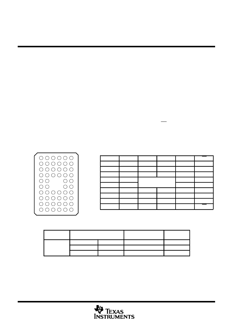
terminal assignments
1
2
3
4
5
6
A
1DIR
NC
NC
NC
NC
1OE
B
1A2
1A1
GND
GND
1B1
1B2
C
1A4
1A3
VCC
GND
BIAS VCC
GND
1B3
1B4
D
E
1A6
1A5
1B5
1B6
2A8
1A7
1B7
1B8
F
2A1
2A2
2B2
2B1
G
2A3
2A4
GND
GND
2B4
2B3
H
2A5
2A6
VCC
GND
VREF
GND
2B6
2B5
J
2A7
2A8
2B8
2B7
K
2DIR
NC
NC
NC
NC
2OE
NC
–
No internal connection
ORDERING INFORMATION
TA
PACKAGE
ORDERABLE
PART NUMBER
TOP-SIDE
MARKING
TSSOP
–
DGG
Tape and reel
SN74GTLPH16945GR
GTLPH16945
–
40
°
C to 85
°
C
TVSOP
–
DGV
Tape and reel
SN74GTLPH16945VR
GL945
VFBGA
–
GQL
Tape and reel
SN74GTLPH16945KR
GL945
Package drawings, standard packing quantities, thermal data, symbolization, and PCB design guidelines
are available at www.ti.com/sc/package.
GQL PACKAGE
(TOP VIEW)
A
B
C
D
E
F
G
H
J
K
1
2
3
4
5
6
相關(guān)PDF資料 |
PDF描述 |
|---|---|
| SN74H102 | AND-GATE J-K NEGATIVE-EDGE-TRIGGERED FLIP-FLOPS WITH PRESET AND CLEAR |
| SN74H102J | AND-GATE J-K NEGATIVE-EDGE-TRIGGERED FLIP-FLOPS WITH PRESET AND CLEAR |
| SN74H102N | AND-GATE J-K NEGATIVE-EDGE-TRIGGERED FLIP-FLOPS WITH PRESET AND CLEAR |
| SN74HC148DWR | 8-LINE TO 3-LINE PRIORITY ENCODERS |
| SN74HC148DWRE4 | 8-LINE TO 3-LINE PRIORITY ENCODERS |
相關(guān)代理商/技術(shù)參數(shù) |
參數(shù)描述 |
|---|---|
| SN74GTLPH306DGVR | 功能描述:轉(zhuǎn)換 - 電壓電平 8bit LVTTL-GTLP RoHS:否 制造商:Micrel 類型:CML/LVDS/LVPECL to LVCMOS/LVTTL 傳播延遲時間:1.9 ns 電源電流:14 mA 電源電壓-最大:3.6 V 電源電壓-最小:3 V 最大工作溫度:+ 85 C 安裝風格:SMD/SMT 封裝 / 箱體:MLF-8 |
| SN74GTLPH306DW | 功能描述:轉(zhuǎn)換 - 電壓電平 8-Bit LVTTL-to-GTLP Bus Transceiver RoHS:否 制造商:Micrel 類型:CML/LVDS/LVPECL to LVCMOS/LVTTL 傳播延遲時間:1.9 ns 電源電流:14 mA 電源電壓-最大:3.6 V 電源電壓-最小:3 V 最大工作溫度:+ 85 C 安裝風格:SMD/SMT 封裝 / 箱體:MLF-8 |
| SN74GTLPH306DWG4 | 功能描述:轉(zhuǎn)換 - 電壓電平 8B LVTTL to GTLP Bus Transceiver RoHS:否 制造商:Micrel 類型:CML/LVDS/LVPECL to LVCMOS/LVTTL 傳播延遲時間:1.9 ns 電源電流:14 mA 電源電壓-最大:3.6 V 電源電壓-最小:3 V 最大工作溫度:+ 85 C 安裝風格:SMD/SMT 封裝 / 箱體:MLF-8 |
| SN74GTLPH306DWR | 功能描述:轉(zhuǎn)換 - 電壓電平 8bit LVTTL-GTLP RoHS:否 制造商:Micrel 類型:CML/LVDS/LVPECL to LVCMOS/LVTTL 傳播延遲時間:1.9 ns 電源電流:14 mA 電源電壓-最大:3.6 V 電源電壓-最小:3 V 最大工作溫度:+ 85 C 安裝風格:SMD/SMT 封裝 / 箱體:MLF-8 |
| SN74GTLPH306DWRE4 | 功能描述:轉(zhuǎn)換 - 電壓電平 Triple 2-Ch Analog Mltplxr/Demltplxr RoHS:否 制造商:Micrel 類型:CML/LVDS/LVPECL to LVCMOS/LVTTL 傳播延遲時間:1.9 ns 電源電流:14 mA 電源電壓-最大:3.6 V 電源電壓-最小:3 V 最大工作溫度:+ 85 C 安裝風格:SMD/SMT 封裝 / 箱體:MLF-8 |
發(fā)布緊急采購,3分鐘左右您將得到回復(fù)。