- 您現(xiàn)在的位置:買賣IC網(wǎng) > PDF目錄374866 > SN74CBTS6800DBQ (Texas Instruments, Inc.) 10-BIT FET BUS SWITCH WITH PRECHARGED OUTPUTS AND SCHOTTKY DIODE CLAMPING PDF資料下載
參數(shù)資料
| 型號: | SN74CBTS6800DBQ |
| 廠商: | Texas Instruments, Inc. |
| 英文描述: | 10-BIT FET BUS SWITCH WITH PRECHARGED OUTPUTS AND SCHOTTKY DIODE CLAMPING |
| 中文描述: | 10位FET總線開關(guān)與預(yù)充電輸出和肖特基二極管鉗位 |
| 文件頁數(shù): | 2/4頁 |
| 文件大小: | 57K |
| 代理商: | SN74CBTS6800DBQ |
SN74CBTS6800
10-BIT FET BUS SWITCH
WITH PRECHARGED OUTPUTS AND SCHOTTKY DIODE CLAMPING
SCDS102A – JUNE 1999 – REVISED JULY 1999
2
POST OFFICE BOX 655303
DALLAS, TEXAS 75265
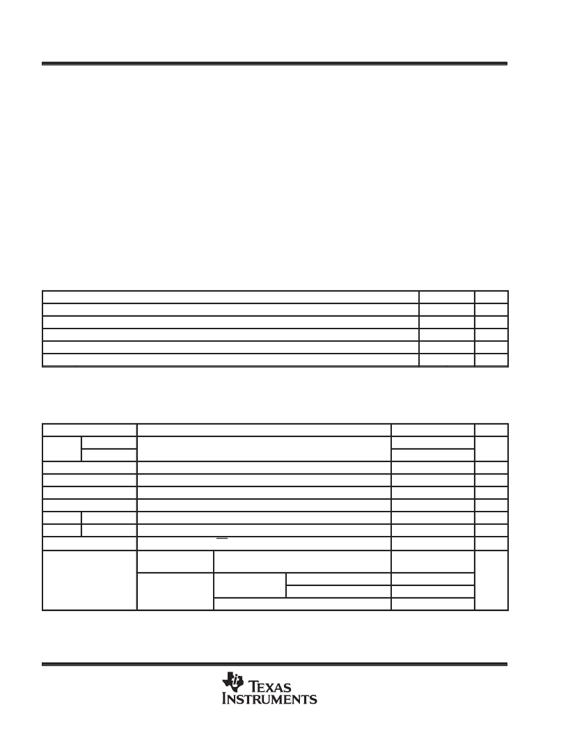
absolute maximum ratings over operating free-air temperature range (unless otherwise noted)
Supply voltage range, V
CC
Bias voltage range, BIASV
Input voltage range, V
I
(see Note 1)
Continuous channel current
Input clamp current, I
IK
(V
I
< 0)
Package thermal impedance,
θ
JA
(see Note 2): DB package
–0.5 V to 7 V
–0.5 V to 7 V
–0.5 V to 7 V
128 mA
–50 mA
104
°
C/W
103
°
C/W
139
°
C/W
81
°
C/W
120
°
C/W
–65
°
C to 150
°
C
. . . . . . . . . . . . . . . . . . . . . . . . . . . . . . . . . . . . . . . . . . . . . . . . . . . . . . . . . .
. . . . . . . . . . . . . . . . . . . . . . . . . . . . . . . . . . . . . . . . . . . . . . . . . . . . . . . . . .
. . . . . . . . . . . . . . . . . . . . . . . . . . . . . . . . . . . . . . . . . . . . . . . . . .
. . . . . . . . . . . . . . . . . . . . . . . . . . . . . . . . . . . . . . . . . . . . . . . . . . . . . . . . . . . . . .
. . . . . . . . . . . . . . . . . . . . . . . . . . . . . . . . . . . . . . . . . . . . . . . . . . . . . . . . . . .
. . . . . . . . . . . . . . . . . . . . . . . . . . . . . . . .
DBQ package
. . . . . . . . . . . . . . . . . . . . . . . . . . . . . . .
DGV package
. . . . . . . . . . . . . . . . . . . . . . . . . . . . . . .
DW package
. . . . . . . . . . . . . . . . . . . . . . . . . . . . . . . . .
PW package
. . . . . . . . . . . . . . . . . . . . . . . . . . . . . . . .
Storage temperature range, T
stg
. . . . . . . . . . . . . . . . . . . . . . . . . . . . . . . . . . . . . . . . . . . . . . . . . . .
Stresses beyond those listed under “absolute maximum ratings” may cause permanent damage to the device. These are stress ratings only, and
functional operation of the device at these or any other conditions beyond those indicated under “recommended operating conditions” is not
implied. Exposure to absolute-maximum-rated conditions for extended periods may affect device reliability.
NOTES:
1. The input and output negative-voltage ratings may be exceeded if the input and output clamp-current ratings are observed.
2. The package thermal impedance is calculated in accordance with JESD 51.
recommended operating conditions (see Note 3)
MIN
MAX
UNIT
VCC
BIASV
Supply voltage
4
5.5
V
Supply voltage
1.3
VCC
V
VIH
VIL
TA
High-level control input voltage
2
V
Low-level control input voltage
0.8
V
°
C
Operating free-air temperature
–40
85
NOTE 3: All unused control inputs of the device must be held at VCC or GND to ensure proper device operation. Refer to the TI application report,
Implications of Slow or Floating CMOS Inputs literature number SCBA004.
electrical characteristics over recommended operating free-air temperature range (unless
otherwise noted)
PARAMETER
A or B inputs
TEST CONDITIONS
MIN
TYP
MAX
–0.7
UNIT
VIK
VCC= 4 5 V
VCC = 4.5 V,
II= 18 mA
II = –18 mA
V
Control inputs
–1.2
IIL
IIH
IO
ICC
ICC§
Ci
Cio(OFF)
VCC = 5.5 V,
VCC = 5.5 V,
VCC = 4.5 V,
VCC = 5.5 V,
VCC = 5.5 V,
VI = 3 V or 0
VO = 3 V or 0,
VCC = 4 V,
TYP at VCC = 4 V
VI = GND
VI = 5.5 V
BIASV = 2.4 V,
–5
μ
A
μ
A
mA
μ
A
mA
150
VO= 0
VI = VCC or GND
Other inputs at VCC or GND
0.25
IO = 0,
One input at 3.4 V,
3
Control inputs
2.5
Control inputs
3.5
pF
ON = VCC
4.5
pF
VI = 2.4 V,
II = 15 mA
11
20
ron
VI= 0
VI = 0
II = 64 mA
II = 30 mA
II = 15 mA
3
7
VCC = 4.5 V
3
6
7
VI = 2.4 V,
15
All typical values are at VCC = 5 V (unless otherwise noted), TA = 25
°
C.
§This is the increase in supply current for each input that is at the specified TTL voltage level rather than VCC or GND.
Measured by the voltage drop between the A and B terminals at the indicated current through the switch. On-state resistance is determined by
the lower of the voltages of the two (A or B) terminals.
相關(guān)PDF資料 |
PDF描述 |
|---|---|
| SN74CBTS6800DGV | 10-BIT FET BUS SWITCH WITH PRECHARGED OUTPUTS AND SCHOTTKY DIODE CLAMPING |
| SN74CBTS6800PW | 10-BIT FET BUS SWITCH WITH PRECHARGED OUTPUTS AND SCHOTTKY DIODE CLAMPING |
| SN74FB2033KRCR | 8-BIT TTL/BTL REGISTERED TRANSCEIVER |
| SN74FB2040RCR | 8-BIT TTL/BTL TRANSCEIVER |
| SN74FB2040RCRG3N | 8-BIT TTL/BTL TRANSCEIVER |
相關(guān)代理商/技術(shù)參數(shù) |
參數(shù)描述 |
|---|---|
| SN74CBTS6800DBQR | 功能描述:數(shù)字總線開關(guān) IC 10bit w/Schotky Clmp RoHS:否 制造商:Texas Instruments 開關(guān)數(shù)量:24 傳播延遲時間:0.25 ns 最大工作溫度:+ 85 C 最小工作溫度:- 40 C 封裝 / 箱體:TSSOP-56 封裝:Reel |
| SN74CBTS6800DBR | 功能描述:數(shù)字總線開關(guān) IC 10-Bit FET Bus Switch RoHS:否 制造商:Texas Instruments 開關(guān)數(shù)量:24 傳播延遲時間:0.25 ns 最大工作溫度:+ 85 C 最小工作溫度:- 40 C 封裝 / 箱體:TSSOP-56 封裝:Reel |
| SN74CBTS6800DBRE4 | 功能描述:數(shù)字總線開關(guān) IC Dual 2 to 4-Line Decoder/Demltplxr RoHS:否 制造商:Texas Instruments 開關(guān)數(shù)量:24 傳播延遲時間:0.25 ns 最大工作溫度:+ 85 C 最小工作溫度:- 40 C 封裝 / 箱體:TSSOP-56 封裝:Reel |
| SN74CBTS6800DBRG4 | 功能描述:數(shù)字總線開關(guān) IC 10B FETBus Switch RoHS:否 制造商:Texas Instruments 開關(guān)數(shù)量:24 傳播延遲時間:0.25 ns 最大工作溫度:+ 85 C 最小工作溫度:- 40 C 封裝 / 箱體:TSSOP-56 封裝:Reel |
| SN74CBTS6800DGVR | 功能描述:數(shù)字總線開關(guān) IC 10bit w/Schotky Clmp RoHS:否 制造商:Texas Instruments 開關(guān)數(shù)量:24 傳播延遲時間:0.25 ns 最大工作溫度:+ 85 C 最小工作溫度:- 40 C 封裝 / 箱體:TSSOP-56 封裝:Reel |
發(fā)布緊急采購,3分鐘左右您將得到回復(fù)。