- 您現(xiàn)在的位置:買賣IC網(wǎng) > PDF目錄374861 > SN74ACT3638PCB (Texas Instruments, Inc.) 512 】 32 】 2 CLOCKED BIDIRECTIONAL FIRST-IN, FIRST-OUT MEMORY PDF資料下載
參數(shù)資料
| 型號: | SN74ACT3638PCB |
| 廠商: | Texas Instruments, Inc. |
| 英文描述: | 512 】 32 】 2 CLOCKED BIDIRECTIONAL FIRST-IN, FIRST-OUT MEMORY |
| 中文描述: | 512】32】2時鐘雙向先入先出存儲器 |
| 文件頁數(shù): | 26/30頁 |
| 文件大?。?/td> | 461K |
| 代理商: | SN74ACT3638PCB |
第1頁第2頁第3頁第4頁第5頁第6頁第7頁第8頁第9頁第10頁第11頁第12頁第13頁第14頁第15頁第16頁第17頁第18頁第19頁第20頁第21頁第22頁第23頁第24頁第25頁當前第26頁第27頁第28頁第29頁第30頁
SN74ACT3638
512
×
32
×
2
CLOCKED BIDIRECTIONAL FIRST-IN, FIRST-OUT MEMORY
SCAS228D – JUNE 1992 – REVISED APRIL 1998
26
POST OFFICE BOX 655303
DALLAS, TEXAS 75265
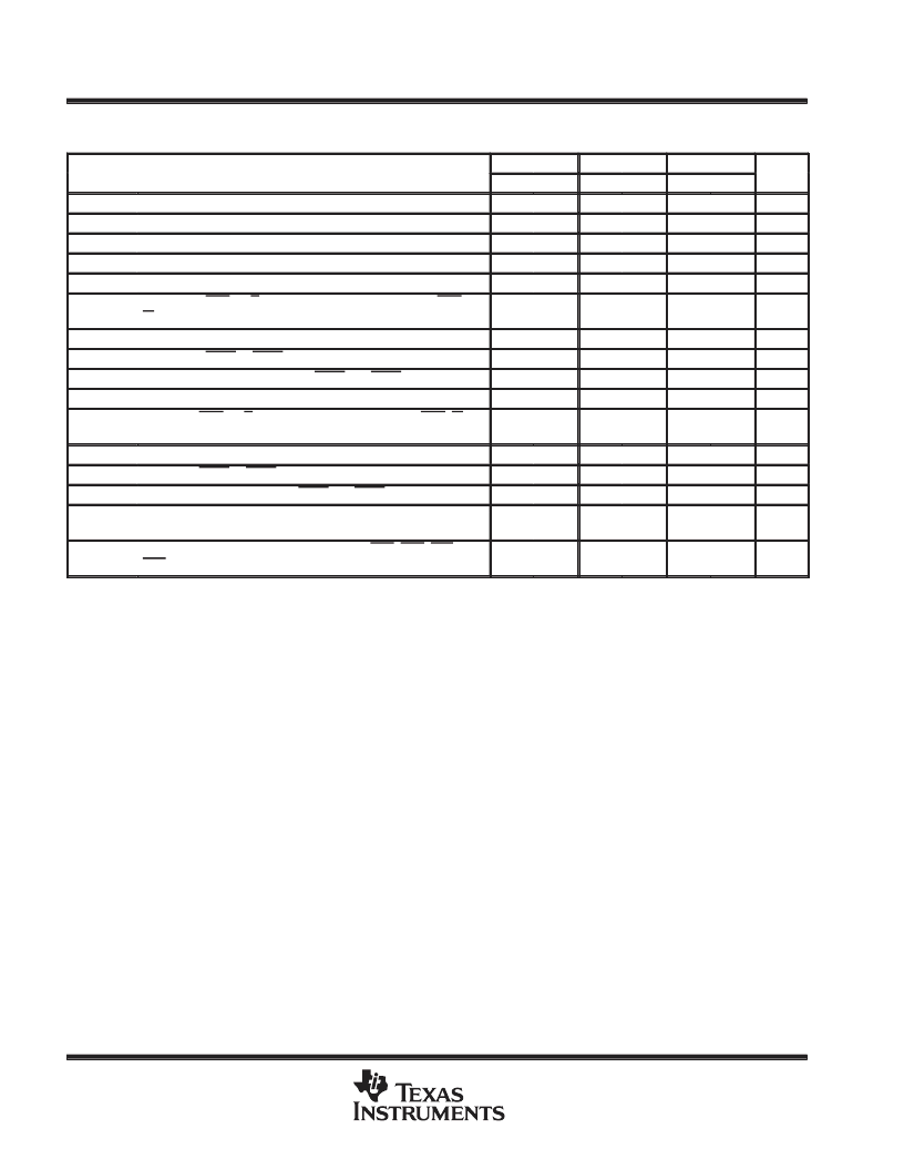
timing requirements over recommended ranges of supply voltage and operating free-air
temperature (see Figures 1 through 23)
’ACT3638-15
MIN
’ACT3638-20
MIN
’ACT3638-30
MIN
UNIT
MAX
MAX
MAX
fclock
tc
tw(CLKH)
tw(CLKL)
tsu(D)
Clock frequency, CLKA or CLKB
66.7
50
33.4
MHz
Clock cycle time, CLKA or CLKB
15
20
30
ns
Pulse duration, CLKA and CLKB high
6
8
10
ns
Pulse duration, CLKA and CLKB low
Setup time, A0–A31 before CLKA
↑
and B0–B31 before CLKB
↑
Setup time, CSA, W/RA, ENA, and MBA before CLKA
↑
; CSB,
W/RB, ENB, and MBB before CLKB
↑
Setup time, RTM and RFM before CLKB
↑
Setup time, RST1 or RST2 low before CLKA
↑
or CLKB
↑
Setup time, FS0 and FS1 before RST1 and RST2 high
Hold time, A0–A31 after CLKA
↑
and B0–B31 after CLKB
↑
Hold time, CSA, W/RA, ENA, and MBA after CLKA
↑
; CSB, W/
RB, ENB, and MBB after CLKB
↑
Hold time, RTM and RFM after CLKB
↑
Hold time, RST1 or RST2 low after CLKA
↑
or CLKB
↑
Hold time, FS0 and FS1 after RST1 and RST2 high
Skew time between CLKA
↑
and CLKB
↑
for ORA, ORB, IRA, and
IRB
Skew time between CLKA
↑
and CLKB
↑
for AEA, AEB, AFA, and
AFB
Requirement to count the clock edge as one of at least four needed to reset a FIFO
Skew time is not a timing constraint for proper device operation and is included only to illustrate the timing relationship between CLKA cycle and
CLKB cycle.
6
8
10
ns
4.5
5
6
ns
tsu(EN)
5
6
7
ns
tsu(RM)
tsu(RS)
tsu(FS)
th(D)
6
6.5
7
ns
5
6
7
ns
7
8
9
ns
0
0
0
ns
th(EN)
0
0
0
ns
th(RM)
th(RS)
th(FS)
0
0
0
ns
4
4
5
ns
2
3
3
ns
tsk1
8
9
11
ns
tsk2
12
16
20
ns
相關PDF資料 |
PDF描述 |
|---|---|
| SN74ACT3638PQ | Low-Voltage Quad 2-Input OR Gate with 5V-Tolerant Inputs; Package: TSSOP-14; No of Pins: 14; Container: Tape and Reel; Qty per Container: 2500 |
| SN74ACT3641PCB | Low-Voltage Quad 2-Input OR Gate with 5V-Tolerant Inputs; Package: SOEIAJ-14; No of Pins: 14; Container: Tape and Reel; Qty per Container: 2000 |
| SN74ACT3641PQ | Low-Voltage Quad 2-Input OR Gate with 5V-Tolerant Inputs, Pb-free; Package: SOEIAJ-14; No of Pins: 14; Container: Tape and Reel; Qty per Container: 2000 |
| SN74ACT3651PCB | Low-Voltage CMOS Octal Transparent Latch; Package: TSSOP 20 LEAD; No of Pins: 20; Container: Rail; Qty per Container: 75 |
| SN74ACT3651PQ | Low-Voltage CMOS Octal Transparent Latch; Package: TSSOP 20 LEAD; No of Pins: 20; Container: Tape and Reel; Qty per Container: 2500 |
相關代理商/技術(shù)參數(shù) |
參數(shù)描述 |
|---|---|
| SN74ACT3641-15PCB | 功能描述:先進先出 1024 x 36 synch 先進先出 Memory RoHS:否 制造商:IDT 電路數(shù)量: 數(shù)據(jù)總線寬度:18 bit 總線定向:Unidirectional 存儲容量:4 Mbit 定時類型:Synchronous 組織:256 K x 18 最大時鐘頻率:100 MHz 訪問時間:10 ns 電源電壓-最大:3.6 V 電源電壓-最小:6 V 最大工作電流:35 mA 最大工作溫度:+ 85 C 封裝 / 箱體:TQFP-80 封裝: |
| SN74ACT3641-15PQ | 功能描述:先進先出 1024 x 36 synch 先進先出 Memory RoHS:否 制造商:IDT 電路數(shù)量: 數(shù)據(jù)總線寬度:18 bit 總線定向:Unidirectional 存儲容量:4 Mbit 定時類型:Synchronous 組織:256 K x 18 最大時鐘頻率:100 MHz 訪問時間:10 ns 電源電壓-最大:3.6 V 電源電壓-最小:6 V 最大工作電流:35 mA 最大工作溫度:+ 85 C 封裝 / 箱體:TQFP-80 封裝: |
| SN74ACT3641-20PCB | 功能描述:先進先出 1024 x 36 synch 先進先出 Memory RoHS:否 制造商:IDT 電路數(shù)量: 數(shù)據(jù)總線寬度:18 bit 總線定向:Unidirectional 存儲容量:4 Mbit 定時類型:Synchronous 組織:256 K x 18 最大時鐘頻率:100 MHz 訪問時間:10 ns 電源電壓-最大:3.6 V 電源電壓-最小:6 V 最大工作電流:35 mA 最大工作溫度:+ 85 C 封裝 / 箱體:TQFP-80 封裝: |
| SN74ACT3641-20PQ | 功能描述:先進先出 1024 x 36 synch 先進先出 Memory RoHS:否 制造商:IDT 電路數(shù)量: 數(shù)據(jù)總線寬度:18 bit 總線定向:Unidirectional 存儲容量:4 Mbit 定時類型:Synchronous 組織:256 K x 18 最大時鐘頻率:100 MHz 訪問時間:10 ns 電源電壓-最大:3.6 V 電源電壓-最小:6 V 最大工作電流:35 mA 最大工作溫度:+ 85 C 封裝 / 箱體:TQFP-80 封裝: |
| SN74ACT3641-30PCB | 功能描述:先進先出 1024 x 36 synch 先進先出 Memory RoHS:否 制造商:IDT 電路數(shù)量: 數(shù)據(jù)總線寬度:18 bit 總線定向:Unidirectional 存儲容量:4 Mbit 定時類型:Synchronous 組織:256 K x 18 最大時鐘頻率:100 MHz 訪問時間:10 ns 電源電壓-最大:3.6 V 電源電壓-最小:6 V 最大工作電流:35 mA 最大工作溫度:+ 85 C 封裝 / 箱體:TQFP-80 封裝: |
發(fā)布緊急采購,3分鐘左右您將得到回復。