- 您現(xiàn)在的位置:買賣IC網(wǎng) > PDF目錄374861 > SN74ACT3638PCB (Texas Instruments, Inc.) 512 】 32 】 2 CLOCKED BIDIRECTIONAL FIRST-IN, FIRST-OUT MEMORY PDF資料下載
參數(shù)資料
| 型號(hào): | SN74ACT3638PCB |
| 廠商: | Texas Instruments, Inc. |
| 英文描述: | 512 】 32 】 2 CLOCKED BIDIRECTIONAL FIRST-IN, FIRST-OUT MEMORY |
| 中文描述: | 512】32】2時(shí)鐘雙向先入先出存儲(chǔ)器 |
| 文件頁數(shù): | 19/30頁 |
| 文件大小: | 461K |
| 代理商: | SN74ACT3638PCB |
第1頁第2頁第3頁第4頁第5頁第6頁第7頁第8頁第9頁第10頁第11頁第12頁第13頁第14頁第15頁第16頁第17頁第18頁當(dāng)前第19頁第20頁第21頁第22頁第23頁第24頁第25頁第26頁第27頁第28頁第29頁第30頁
SN74ACT3638
512
×
32
×
2
CLOCKED BIDIRECTIONAL FIRST-IN, FIRST-OUT MEMORY
SCAS228D – JUNE 1992 – REVISED APRIL 1998
19
POST OFFICE BOX 655303
DALLAS, TEXAS 75265
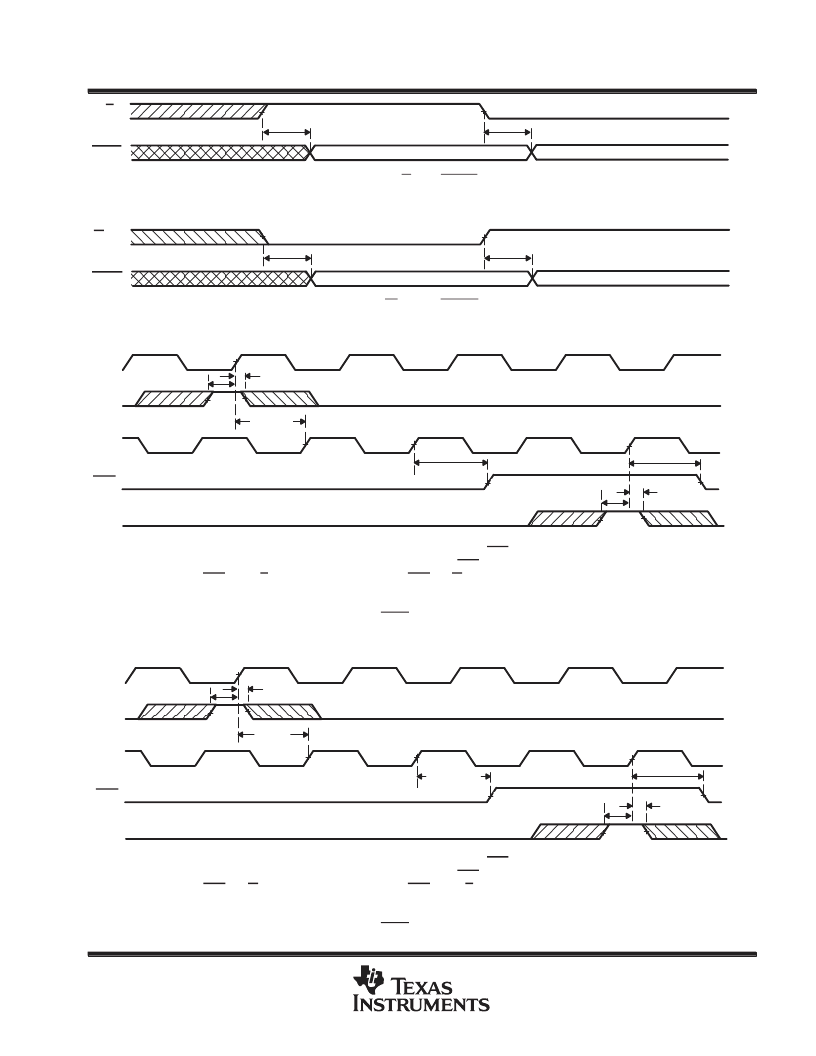
tpd(W-R)
W/RA
RDYA
Inverse of ORA
Inverse of IRA
tpd(W-R)
Figure 11. W/RA to RDYA Timing
ìììììììì
tpd(W-R)
W/RB
RDYB
Inverse of ORB
Inverse of IRB
tpd(W-R)
Figure 12. W/RB to RDYB Timing
tpd(C-AE)
tsu(EN)
CLKA
AEB
ENB
ENA
th(EN)
tsu(EN)
tsk2
X1 Words in FIFO1
1
CLKB
2
tpd(C-AE)
ììììì
(X1 + 1) Words in FIFO1
ììììì
ììììì
tsk2 is the minimum time between a rising CLKA edge and a rising CLKB edge for AEB to transition high in the next CLKB cycle. If the time
between the rising CLKA edge and rising CLKB edge is less than tsk2, then AEB may transition high one CLKB cycle later than shown.
NOTE A: FIFO1 write (CSA = L, W/RA = H, MBA = L), FIFO1 read (CSB = L, W/RB = H, MBB = L). Data in the FIFO1 output register has been
read from the FIFO.
Figure 13. Timing for AEB When FIFO1 Is Almost Empty
tsu(EN)
CLKB
AEA
ENA
ENB
th(EN)
tsu(EN)
tpd(C-AE)
X2 Words in FIFO2
1
CLKA
2
tpd(C-AE)
th(EN)
ììììì
ììììì
(X2 + 1) Words in FIFO2
ììììì
tsk2 is the minimum time between a rising CLKB edge and a rising CLKA edge for AEA to transition high in the next CLKA cycle. If the time
between the rising CLKB edge and rising CLKA edge is less than tsk2, then AEA may transition high one CLKA cycle later than shown.
NOTE A: FIFO2 write (CSB = L, W/RB = L, MBB = L), FIFO2 read (CSA = L, W/RA = L, MBA = L). Data in the FIFO2 output register has been
read from the FIFO.
Figure 14. Timing for AEA When FIFO2 Is Almost Empty
相關(guān)PDF資料 |
PDF描述 |
|---|---|
| SN74ACT3638PQ | Low-Voltage Quad 2-Input OR Gate with 5V-Tolerant Inputs; Package: TSSOP-14; No of Pins: 14; Container: Tape and Reel; Qty per Container: 2500 |
| SN74ACT3641PCB | Low-Voltage Quad 2-Input OR Gate with 5V-Tolerant Inputs; Package: SOEIAJ-14; No of Pins: 14; Container: Tape and Reel; Qty per Container: 2000 |
| SN74ACT3641PQ | Low-Voltage Quad 2-Input OR Gate with 5V-Tolerant Inputs, Pb-free; Package: SOEIAJ-14; No of Pins: 14; Container: Tape and Reel; Qty per Container: 2000 |
| SN74ACT3651PCB | Low-Voltage CMOS Octal Transparent Latch; Package: TSSOP 20 LEAD; No of Pins: 20; Container: Rail; Qty per Container: 75 |
| SN74ACT3651PQ | Low-Voltage CMOS Octal Transparent Latch; Package: TSSOP 20 LEAD; No of Pins: 20; Container: Tape and Reel; Qty per Container: 2500 |
相關(guān)代理商/技術(shù)參數(shù) |
參數(shù)描述 |
|---|---|
| SN74ACT3641-15PCB | 功能描述:先進(jìn)先出 1024 x 36 synch 先進(jìn)先出 Memory RoHS:否 制造商:IDT 電路數(shù)量: 數(shù)據(jù)總線寬度:18 bit 總線定向:Unidirectional 存儲(chǔ)容量:4 Mbit 定時(shí)類型:Synchronous 組織:256 K x 18 最大時(shí)鐘頻率:100 MHz 訪問時(shí)間:10 ns 電源電壓-最大:3.6 V 電源電壓-最小:6 V 最大工作電流:35 mA 最大工作溫度:+ 85 C 封裝 / 箱體:TQFP-80 封裝: |
| SN74ACT3641-15PQ | 功能描述:先進(jìn)先出 1024 x 36 synch 先進(jìn)先出 Memory RoHS:否 制造商:IDT 電路數(shù)量: 數(shù)據(jù)總線寬度:18 bit 總線定向:Unidirectional 存儲(chǔ)容量:4 Mbit 定時(shí)類型:Synchronous 組織:256 K x 18 最大時(shí)鐘頻率:100 MHz 訪問時(shí)間:10 ns 電源電壓-最大:3.6 V 電源電壓-最小:6 V 最大工作電流:35 mA 最大工作溫度:+ 85 C 封裝 / 箱體:TQFP-80 封裝: |
| SN74ACT3641-20PCB | 功能描述:先進(jìn)先出 1024 x 36 synch 先進(jìn)先出 Memory RoHS:否 制造商:IDT 電路數(shù)量: 數(shù)據(jù)總線寬度:18 bit 總線定向:Unidirectional 存儲(chǔ)容量:4 Mbit 定時(shí)類型:Synchronous 組織:256 K x 18 最大時(shí)鐘頻率:100 MHz 訪問時(shí)間:10 ns 電源電壓-最大:3.6 V 電源電壓-最小:6 V 最大工作電流:35 mA 最大工作溫度:+ 85 C 封裝 / 箱體:TQFP-80 封裝: |
| SN74ACT3641-20PQ | 功能描述:先進(jìn)先出 1024 x 36 synch 先進(jìn)先出 Memory RoHS:否 制造商:IDT 電路數(shù)量: 數(shù)據(jù)總線寬度:18 bit 總線定向:Unidirectional 存儲(chǔ)容量:4 Mbit 定時(shí)類型:Synchronous 組織:256 K x 18 最大時(shí)鐘頻率:100 MHz 訪問時(shí)間:10 ns 電源電壓-最大:3.6 V 電源電壓-最小:6 V 最大工作電流:35 mA 最大工作溫度:+ 85 C 封裝 / 箱體:TQFP-80 封裝: |
| SN74ACT3641-30PCB | 功能描述:先進(jìn)先出 1024 x 36 synch 先進(jìn)先出 Memory RoHS:否 制造商:IDT 電路數(shù)量: 數(shù)據(jù)總線寬度:18 bit 總線定向:Unidirectional 存儲(chǔ)容量:4 Mbit 定時(shí)類型:Synchronous 組織:256 K x 18 最大時(shí)鐘頻率:100 MHz 訪問時(shí)間:10 ns 電源電壓-最大:3.6 V 電源電壓-最小:6 V 最大工作電流:35 mA 最大工作溫度:+ 85 C 封裝 / 箱體:TQFP-80 封裝: |
發(fā)布緊急采購,3分鐘左右您將得到回復(fù)。