- 您現(xiàn)在的位置:買(mǎi)賣(mài)IC網(wǎng) > PDF目錄374861 > SN54ABT821FK (Texas Instruments, Inc.) 10-BIT BUS-INTERFACE FLIP-FLOPS WITH 3-STATE OUTPUTS PDF資料下載
參數(shù)資料
| 型號(hào): | SN54ABT821FK |
| 廠商: | Texas Instruments, Inc. |
| 英文描述: | 10-BIT BUS-INTERFACE FLIP-FLOPS WITH 3-STATE OUTPUTS |
| 中文描述: | 10位總線接口倒裝3觸發(fā)器態(tài)輸出 |
| 文件頁(yè)數(shù): | 3/7頁(yè) |
| 文件大?。?/td> | 108K |
| 代理商: | SN54ABT821FK |
SN54ABT821, SN74ABT821A
10-BIT BUS-INTERFACE FLIP-FLOPS
WITH 3-STATE OUTPUTS
SCBS193E – FEBRUARY 1991 – REVISED MAY 1997
3
POST OFFICE BOX 655303
DALLAS, TEXAS 75265
absolute maximum ratings over operating free-air temperature range (unless otherwise noted)
Supply voltage range, V
CC
Input voltage range, V
I
(see Note 1)
Voltage range applied to any output in the high or power-off state, V
O
Current into any output in the low state, I
O
: SN54ABT821
–0.5 V to 7 V
–0.5 V to 7 V
–0.5 V to 5.5 V
. . . . . . . . . . . . . . . . . . . . . . . . . . . . . . . . . . . . . . . . . . . . . . . . . . . . . . . . . .
. . . . . . . . . . . . . . . . . . . . . . . . . . . . . . . . . . . . . . . . . . . . . . . . . .
. . . . . . . . . . . . . . . . . . .
96 mA
128 mA
–18 mA
–50 mA
104
°
C/W
81
°
C/W
67
°
C/W
. . . . . . . . . . . . . . . . . . . . . . . . . . . . . . . . . . . .
. . . . . . . . . . . . . . . . . . . . . . . . . . . . . . . . . .
SN74ABT821A
Input clamp current, I
IK
(V
I
< 0)
Output clamp current, I
OK
(V
O
< 0)
Package thermal impedance,
θ
JA
(see Note 2): DB package
. . . . . . . . . . . . . . . . . . . . . . . . . . . . . . . . . . . . . . . . . . . . . . . . . . . . . . . . . . .
. . . . . . . . . . . . . . . . . . . . . . . . . . . . . . . . . . . . . . . . . . . . . . . . . . . . . . . .
. . . . . . . . . . . . . . . . . . . . . . . . . . . . . . . .
DW package
. . . . . . . . . . . . . . . . . . . . . . . . . . . . . . . . .
NT package
. . . . . . . . . . . . . . . . . . . . . . . . . . . . . . . . .
. . . . . . . . . . . . . . . . . . . . . . . . . . . . . . . . . . . . . . . . . . . . . . . . . . .
Storage temperature range, T
stg
Stresses beyond those listed under “absolute maximum ratings” may cause permanent damage to the device. These are stress ratings only, and
functional operation of the device at these or any other conditions beyond those indicated under “recommended operating conditions” is not
implied. Exposure to absolute-maximum-rated conditions for extended periods may affect device reliability.
NOTES:
1. The input and output negative-voltage ratings may be exceeded if the input and output clamp-current ratings are observed.
2. The package thermal impedance is calculated in accordance with EIA/JEDEC Std JESD51, except for through-hole packages,
which use a trace length of zero.
–65
°
C to 150
°
C
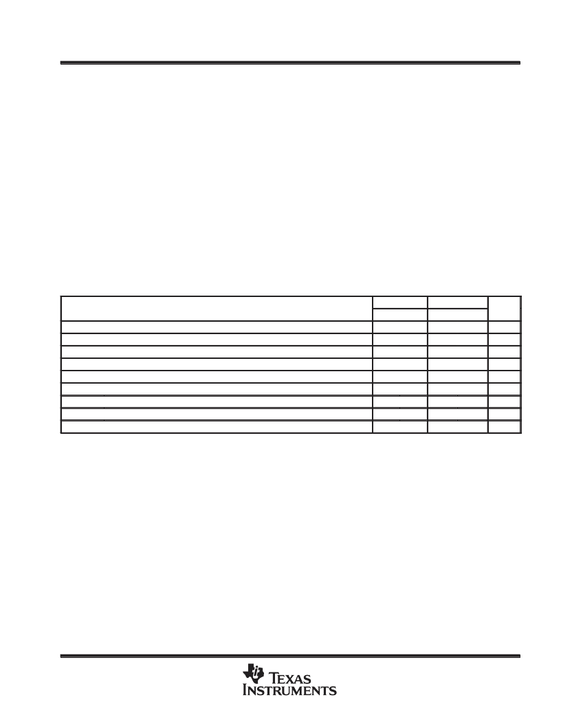
recommended operating conditions (see Note 3)
SN54ABT821
MIN
SN74ABT821A
MIN
UNIT
MAX
MAX
VCC
VIH
VIL
VI
IOH
IOL
t/
v
t/
VCC
TA
NOTE 3: Unused inputs must be held high or low to prevent them from floating.
Supply voltage
4.5
5.5
4.5
5.5
V
High-level input voltage
2
2
V
Low-level input voltage
0.8
0.8
V
Input voltage
0
VCC
–24
0
VCC
–32
V
High-level output current
mA
Low-level output current
48
64
mA
Input transition rise or fall rate
10
10
ns/V
μ
s/V
°
C
Power-up ramp rate
200
200
Operating free-air temperature
–55
125
–40
85
相關(guān)PDF資料 |
PDF描述 |
|---|---|
| SN54ABT821JT | 10-BIT BUS-INTERFACE FLIP-FLOPS WITH 3-STATE OUTPUTS |
| SN54ABT821W | 10-BIT BUS-INTERFACE FLIP-FLOPS WITH 3-STATE OUTPUTS |
| SN74ABT823DB | 9-BIT BUS-INTERFACE FLIP-FLOPS WITH 3-STATE OUTPUTS |
| SN54ABT823FK | 9-BIT BUS-INTERFACE FLIP-FLOPS WITH 3-STATE OUTPUTS |
| SN54ABT823JT | 9-BIT BUS-INTERFACE FLIP-FLOPS WITH 3-STATE OUTPUTS |
相關(guān)代理商/技術(shù)參數(shù) |
參數(shù)描述 |
|---|---|
| SN54ABT821JT | 制造商:TI 制造商全稱(chēng):Texas Instruments 功能描述:10-BIT BUS-INTERFACE FLIP-FLOPS WITH 3-STATE OUTPUTS |
| SN54ABT821W | 制造商:TI 制造商全稱(chēng):Texas Instruments 功能描述:10-BIT BUS-INTERFACE FLIP-FLOPS WITH 3-STATE OUTPUTS |
| SN54ABT823 | 制造商:TI 制造商全稱(chēng):Texas Instruments 功能描述:9-BIT BUS-INTERFACE FLIP-FLOPS WITH 3-STATE OUTPUTS |
| SN54ABT823FK | 制造商:TI 制造商全稱(chēng):Texas Instruments 功能描述:9-BIT BUS-INTERFACE FLIP-FLOPS WITH 3-STATE OUTPUTS |
| SN54ABT823JT | 制造商:TI 制造商全稱(chēng):Texas Instruments 功能描述:9-BIT BUS-INTERFACE FLIP-FLOPS WITH 3-STATE OUTPUTS |
發(fā)布緊急采購(gòu),3分鐘左右您將得到回復(fù)。