- 您現(xiàn)在的位置:買賣IC網(wǎng) > PDF目錄374835 > SMD-5962-94563 (Electronic Theatre Controls, Inc.) Hybrid - High Reliability DC/DC Converters PDF資料下載
參數(shù)資料
| 型號: | SMD-5962-94563 |
| 廠商: | Electronic Theatre Controls, Inc. |
| 英文描述: | Hybrid - High Reliability DC/DC Converters |
| 中文描述: | 混合-高可靠性的直流/直流轉(zhuǎn)換器 |
| 文件頁數(shù): | 3/14頁 |
| 文件大小: | 185K |
| 代理商: | SMD-5962-94563 |
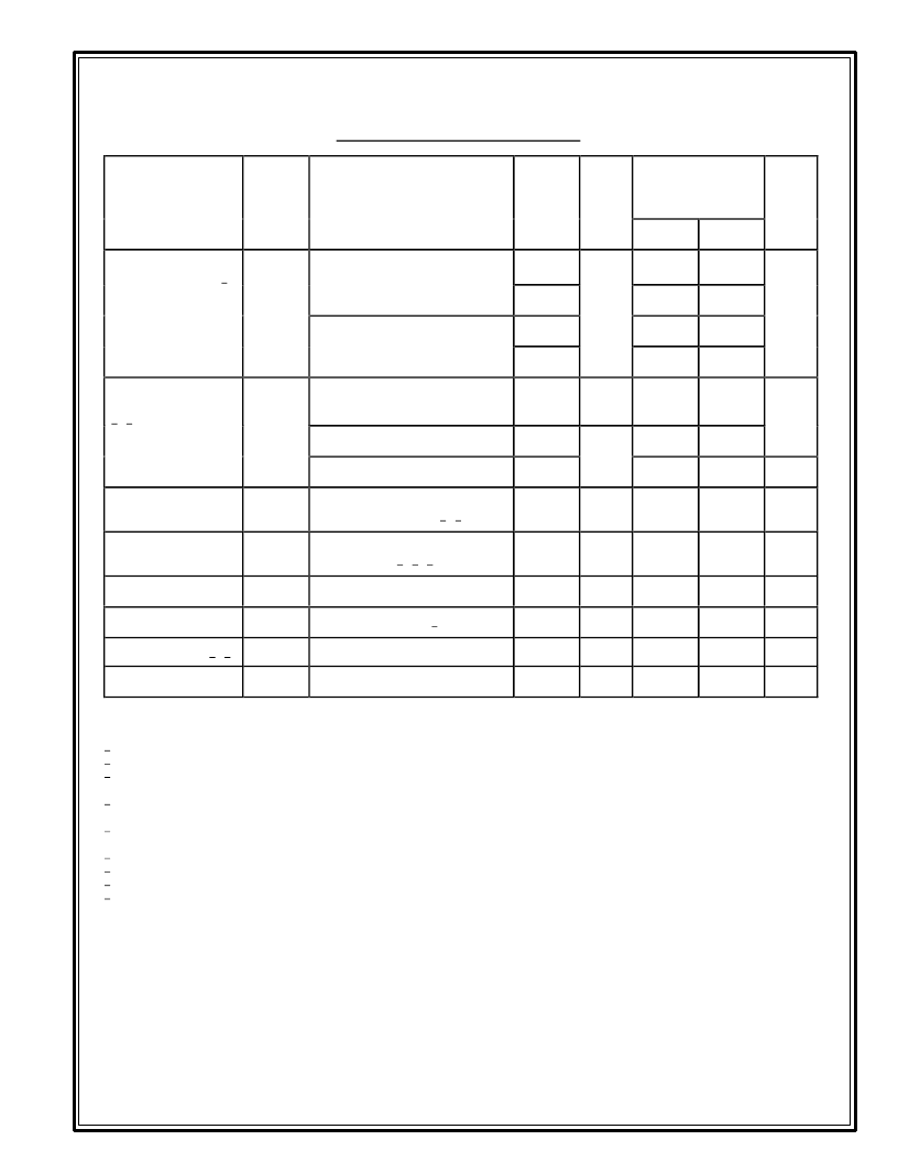
3
AHF2812S
TABLE II. Electrical Performance Characteristics - Continued
Test
Symbol
Conditions
-55
°
C
≤
T
C
≤
+125
°
C
V
IN
= 28 V dc ±5%, C
L
= 0 unless
otherwise specified
Group A
Subgroups
Device
types
Limits
Unit
Min
Max
Output response to step
transient load changes 6/
VO
TLOAD
500 mA to/from 1000 mA
4
01
-300
+300
mV pk
5,6
-450
+450
0 mA to/from 500 mA
4
-500
+500
5,6
-750
+750
Recovery time, step
transient load changes
6/ 7/
TT
LOAD
500 mA to/from 1000 mA
4,5,6
01
100
μs
0 mA to 500 mA
4,5,6
01
1500
500 mA to 0 mA
4,5,6
10
ms
Output response to
transient step line changes
VO
TLINE
Input step 16 V to/from
40 V dc, I
OUT
= 1000 mA 4/ 8/
4,5,6
01
1500
mV pk
Recovery time transient
step line changes
TT
LINE
Input step 16 V to/from 40 V dc
I
OUT
= 1000 mA 4/ 7/ 8/
4,5,6
01
800
μs
Turn on overshoot
VTon
OS
I
OUT
= 0 and 1000 mA
4,5,6
01
600
mV pk
Turn on delay
Ton
D
I
OUT
= 0 and 1000 mA 9/
4,5,6
01
20
ms
Load fault recovery 4/ 9/
Tr
LF
4,5,6
01
20
ms
Weight
35
grams
Notes:
1/ Parameter guaranteed by line and load regulation tests.
2/ Bandwidth guaranteed by design. Tested for 20 kHz to 2 MHz.
3/ Capacitive load may be any value from 0 to the maximum limit without compromising dc performance. A capacitive load in excess of the maximum
limit will not disturb loop stability but may interfere with the operation of the load fault detection circuitry, appearing as a short circuit during turn-on.
4/ Parameter shall be tested as part of design characterization and after design or process changes. Thereafter, parameters shall be guaranteed to the
limits specified in Table II.
5/ An overload is that condition with a load in excess of the rated load but less than that necessary to trigger the short circuit protection and is the
condition of maximum power dissipation.
6/ Load step transition time between 2 and 10 microseconds.
7/ Recovery time is measured from the initiation of the transient to where V
OUT
has returned to within ±1 percent of V
OUT
at 50 percent load.
8/ Input step transition time between 2 and 10 microseconds.
9/ Turn-on delay time measurement is for either a step application of power at the input or the removal of a ground signal from the inhibit pin (pin 1)
while power is applied to the input
is unlimited.
相關(guān)PDF資料 |
PDF描述 |
|---|---|
| SMD-5962-94568 | Hybrid - High Reliability DC/DC Converters |
| SMD030-2 | PolySwitch SMD |
| SMD050-2 | PolySwitch SMD |
| SMD075-2 | PolySwitch SMD |
| SMD100-2 | PolySwitch SMD |
相關(guān)代理商/技術(shù)參數(shù) |
參數(shù)描述 |
|---|---|
| SMD-5962-94568 | 制造商:未知廠家 制造商全稱:未知廠家 功能描述:Hybrid - High Reliability DC/DC Converters |
| SMD5FRA010 | 制造商:Switchcraft 功能描述:SWITCHCRAFT SPECIAL |
| SMD5FRA011 | 制造商:Switchcraft 功能描述:SWITCHCRAFT SPECIAL |
| SMD5FRA020 | 制造商:Switchcraft 功能描述:SWITCHCRAFT SPECIAL |
| SMD5FRA021 | 制造商:Switchcraft 功能描述:SWITCHCRAFT SPECIAL |
發(fā)布緊急采購,3分鐘左右您將得到回復(fù)。