- 您現(xiàn)在的位置:買賣IC網(wǎng) > PDF目錄225180 > SI9939DY-T1 (VISHAY SILICONIX) 3500 mA, 30 V, 2 CHANNEL, N AND P-CHANNEL, Si, SMALL SIGNAL, MOSFET PDF資料下載
參數(shù)資料
| 型號(hào): | SI9939DY-T1 |
| 廠商: | VISHAY SILICONIX |
| 元件分類: | 小信號(hào)晶體管 |
| 英文描述: | 3500 mA, 30 V, 2 CHANNEL, N AND P-CHANNEL, Si, SMALL SIGNAL, MOSFET |
| 文件頁數(shù): | 2/7頁 |
| 文件大小: | 121K |
| 代理商: | SI9939DY-T1 |
Si9939DY
Vishay Siliconix
www.vishay.com
S FaxBack 408-970-5600
2
Document Number: 70146
S-00652—Rev. G, 27-Mar-00
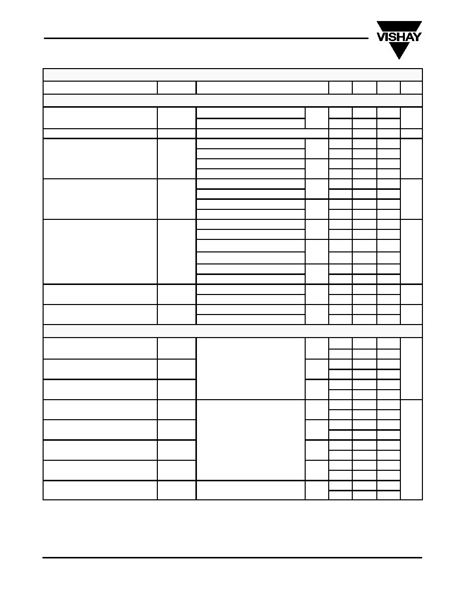
SPECIFICATIONS (TJ = 25_C UNLESS OTHERWISE NOTED)
Parameter
Symbol
Test Condition
Min
Typa
Max
Unit
Static
Gate Threshold Voltage
VGS(th)
VDS = VGS, ID = 250 mA
N-Ch
1.0
V
Gate Threshold Voltage
VGS(th)
VDS = VGS, ID = –250 mA
P-Ch
–1.0
V
Gate-Body Leakage
IGSS
VDS = 0 V, VGS = "20 V
"100
nA
ZG
V l
D i C
I
VDS = 24 V, VGS = 0 V
N-Ch
1
A
Zero Gate Voltage Drain Current
IDSS
VDS = –24 V, VGS = 0 V
P-Ch
–1
mA
Zero Gate Voltage Drain Current
IDSS
VDS = 15 V, VGS = 0 V, TJ = 70_C
N-Ch
5
mA
VDS = –15 V, VGS = 0 V, TJ = 70_C
P-Ch
–5
OS
Di C
b
I
VDS w 5 V, VGS = 10 V
N-Ch
20
A
On-State Drain Currentb
ID(on)
VDS v –5 V, VGS = –10 V
P-Ch
–20
A
On-State Drain Currentb
ID(on)
VDS w 5 V, VGS = 4.5 V
N-Ch
3.5
A
VDS v –5 V, VGS = –4.5 V
P-Ch
–3.5
DiS
OS
R
i
b
VGS = 10 V, ID = 3.5 A
N-Ch
0.04
0.05
W
DiS
OS
R
i
b
VGS = –10 V, ID = 3.5 A
P-Ch
0.074
0.10
W
Drain-Source On-State Resistanceb
rDS(on)
VGS = 6 V, ID = 3 A
N-Ch
0.045
0.07
W
Drain-Source On-State Resistanceb
rDS(on)
VGS = – 6 V, ID = 3 A
P-Ch
0.090
0.12
W
VGS = 4.5 V, ID = 2.5 A
N-Ch
0.054
0.08
VGS = –4.5 V, ID = 2 A
P-Ch
0.115
0.16
Forward Transconductanceb
gfs
VDS = 15 V, ID = 3.5 A
N-Ch
9
S
Forward Transconductanceb
gfs
VDS = –15 V, ID = –3.5 A
P-Ch
6
S
Diode Forward Voltageb
VSD
IS = 1.7 A, VGS = 0 V
N-Ch
0.75
1.2
V
Diode Forward Voltageb
VSD
IS = –1.7 A, VGS = 0 V
P-Ch
–0.75
–1.2
V
Dynamica
Total Gate Charge
Qg
NCh
l
N-Ch
14
35
C
Total Gate Charge
Qg
N-Channel
V
10V V
10V I
3 5 A
P-Ch
14.5
35
C
Gate-Source Charge
Qgs
VDS = 10 V, VGS = 10 V, ID = 3.5 A
N-Ch
1.9
nC
Gate-Source Charge
Qgs
P-Channel
VDS = –10 V, VGS = –10 V
P-Ch
2.7
nC
Gate-Drain Charge
Qgd
VDS = –10 V, VGS = –10 V
ID = –3.5 A
N-Ch
2.8
Gate-Drain Charge
Qgd
P-Ch
3.5
Turn-On Delay Time
td(on)
NCh
l
N-Ch
10
30
Turn-On Delay Time
td(on)
NCh
l
P-Ch
11
30
Rise Time
tr
N-Channel
VDD = 15 V, RL = 15 W
N-Ch
10
40
Rise Time
tr
VDD = 15 V, RL = 15 W
ID ^ 1 A, VGEN = 10 V, RG = 6 W
P-Ch
11
40
Turn-Off Delay Time
td(off)
P-Channel
V15 V R
15
W
N-Ch
26
50
ns
Turn-Off Delay Time
td(off)
VDD = –15 V, RL = 15 W
ID ^ –1 A, VGEN = –10 V, RG = 6 W
P-Ch
30
50
ns
Fall Time
tf
ID
1 A, VGEN
10 V, RG
6
W
N-Ch
10
50
Fall Time
tf
P-Ch
12
50
Source-Drain Reverse Recovery Time
trr
IF = 3.5 A, di/dt = 100 A/ms
N-Ch
60
120
Source-Drain Reverse Recovery Time
trr
IF = 3.5 A, di/dt = 100 A/ms
P-Ch
40
100
Notes
a.
Guaranteed by design, not subject to production testing.
b.
Pulse test; pulse width
v 300 ms, duty cycle v 2%.
相關(guān)PDF資料 |
PDF描述 |
|---|---|
| SI9959DY-T1 | 2000 mA, 60 V, 2 CHANNEL, N-CHANNEL, Si, SMALL SIGNAL, MOSFET |
| SIL30C-12SADJ-VS | 1-OUTPUT DC-DC REG PWR SUPPLY MODULE |
| SIP1X32-301B | IC SOCKET |
| SIP1X32-301B-H | IC SOCKET |
| SIP1X32-300B | IC SOCKET |
相關(guān)代理商/技術(shù)參數(shù) |
參數(shù)描述 |
|---|---|
| SI9940DY | 制造商:TEMIC 制造商全稱:TEMIC Semiconductors 功能描述:DUAL N-CHANNEL ENHANCEMENT-MODE MOSFET |
| SI9942DY | 功能描述:MOSFET 20V 3/2.5A 2W RoHS:否 制造商:STMicroelectronics 晶體管極性:N-Channel 汲極/源極擊穿電壓:650 V 閘/源擊穿電壓:25 V 漏極連續(xù)電流:130 A 電阻汲極/源極 RDS(導(dǎo)通):0.014 Ohms 配置:Single 最大工作溫度: 安裝風(fēng)格:Through Hole 封裝 / 箱體:Max247 封裝:Tube |
| SI9942-DY | 制造商:SIL 功能描述: |
| SI9942DY-T1 | 制造商:Vishay Angstrohm 功能描述:Trans MOSFET N/P-CH 20V 3A/2.5A 8-Pin SOIC N T/R |
| SI9945AEY | 功能描述:MOSFET 60V 3.7A 2.4W RoHS:否 制造商:STMicroelectronics 晶體管極性:N-Channel 汲極/源極擊穿電壓:650 V 閘/源擊穿電壓:25 V 漏極連續(xù)電流:130 A 電阻汲極/源極 RDS(導(dǎo)通):0.014 Ohms 配置:Single 最大工作溫度: 安裝風(fēng)格:Through Hole 封裝 / 箱體:Max247 封裝:Tube |
發(fā)布緊急采購,3分鐘左右您將得到回復(fù)。