- 您現(xiàn)在的位置:買賣IC網(wǎng) > PDF目錄374788 > Si4133-BM (Electronic Theatre Controls, Inc.) DUAL-BAND RF SYNTHESIZER WITH INTEGRATED VCOS FOR WIRELESS COMMUNICATIONS PDF資料下載
參數(shù)資料
| 型號: | Si4133-BM |
| 廠商: | Electronic Theatre Controls, Inc. |
| 英文描述: | DUAL-BAND RF SYNTHESIZER WITH INTEGRATED VCOS FOR WIRELESS COMMUNICATIONS |
| 中文描述: | 雙波段射頻合成器集成的無線通信和VCO |
| 文件頁數(shù): | 18/34頁 |
| 文件大小: | 713K |
| 代理商: | SI4133-BM |
第1頁第2頁第3頁第4頁第5頁第6頁第7頁第8頁第9頁第10頁第11頁第12頁第13頁第14頁第15頁第16頁第17頁當(dāng)前第18頁第19頁第20頁第21頁第22頁第23頁第24頁第25頁第26頁第27頁第28頁第29頁第30頁第31頁第32頁第33頁第34頁
Si4133
18
Rev. 1.1
Applications where the PLL is regularly powered-down
or the frequency is periodically reprogrammed minimize
or eliminate the potential effects of temperature drift
because the VCO is re-tuned in either case. In
applications where the ambient temperature can drift
substantially after self-tuning, it may be necessary to
monitor the lock-detect bar (LDETB) signal on the
AUXOUT pin to determine whether a PLL is about to
run out of locking capability. (See “Auxiliary Output
(AUXOUT)” for how to select LDETB.) The LDETB
signal will be low after self-tuning has completed but will
rise when either the IF or RF PLL nears the limit of its
compensation range. (LDETB will also be high when
either PLL is executing the self-tuning algorithm.) The
output frequency will still be locked when LDETB goes
high, but the PLL will eventually lose lock if the
temperature continues to drift in the same direction.
Therefore, if LDETB goes high both the IF and RF PLLs
should promptly be re-tuned by initiating the self-tuning
algorithm.
Output Frequencies
The IF and RF output frequencies are set by
programming the R- and N-Divider registers. Each PLL
has its own R and N registers so that each can be
programmed independently. Programming either the R-
or N-Divider register for RF1 or RF2 automatically
selects the associated output.
The reference frequency on the XIN pin is divided by R
and this signal is input to the PLL’s phase detector. The
other input to the phase detector is the PLL’s VCO
output frequency divided by N. The PLL acts to make
these frequencies equal. That is, after an initial transient
or
The R values are set by programming the RF1 R-
Divider register (Register 6), the RF2
R-Divider register
(Register 7) and the IF R-Divider register (Register 8).
The N values are set by programming the RF1 N-
Divider register (Register 3), the RF2 N-Divider register
(Register 4), and the IF N-Divider register (Register 5).
Each N-Divider is implemented as a conventional high
speed divider. That is, it consists of a dual-modulus
prescaler, a swallow counter, and a lower speed
synchronous counter. However, the control of these
sub-circuits is handled
appropriate N value should be programmed.
automatically. Only the
PLL Loop Dynamics
The transient response for each PLL is determined by
its phase detector update rate f
φ
(equal to f
REF
/R) and
the phase detector gain programmed for each RF1,
RF2, or IF synthesizer. (See Register 1.) Four different
settings for the phase detector gain are available for
each PLL. The highest gain is programmed by setting
the two phase detector gain bits to 00, and the lowest by
setting the bits to 11. The values of the available gains,
relative to the highest gain, are as follows:
The gain value bits can be automatically set by setting
the Auto K
P
bit (bit 2) in the Main Configuration register
to 1. In setting this bit, the gain values will be optimized
for a given value of N. In general, a higher phase
detector gain will decrease in-band phase noise and
increase the speed of the PLL transient until the point at
which stability begins to be compromised. The optimal
gain depends on N. Table 9 lists recommended settings
for different values of N. These are the settings used
when the Auto K
P
bit is set.
The VCO gain and loop filter characteristics are not
programmable.
The settling time for the PLL is directly proportional to its
phase detector update period T
φ
(T
φ
equals 1/f
φ
). A
typical transient response is shown in Figure 6 on page
11. During the first 13 update periods the Si4133
executes the self-tuning algorithm. Thereafter the PLL
f
N
-----------
f
R
-----------
=
f
OUT
N
R
---
f
REF
=
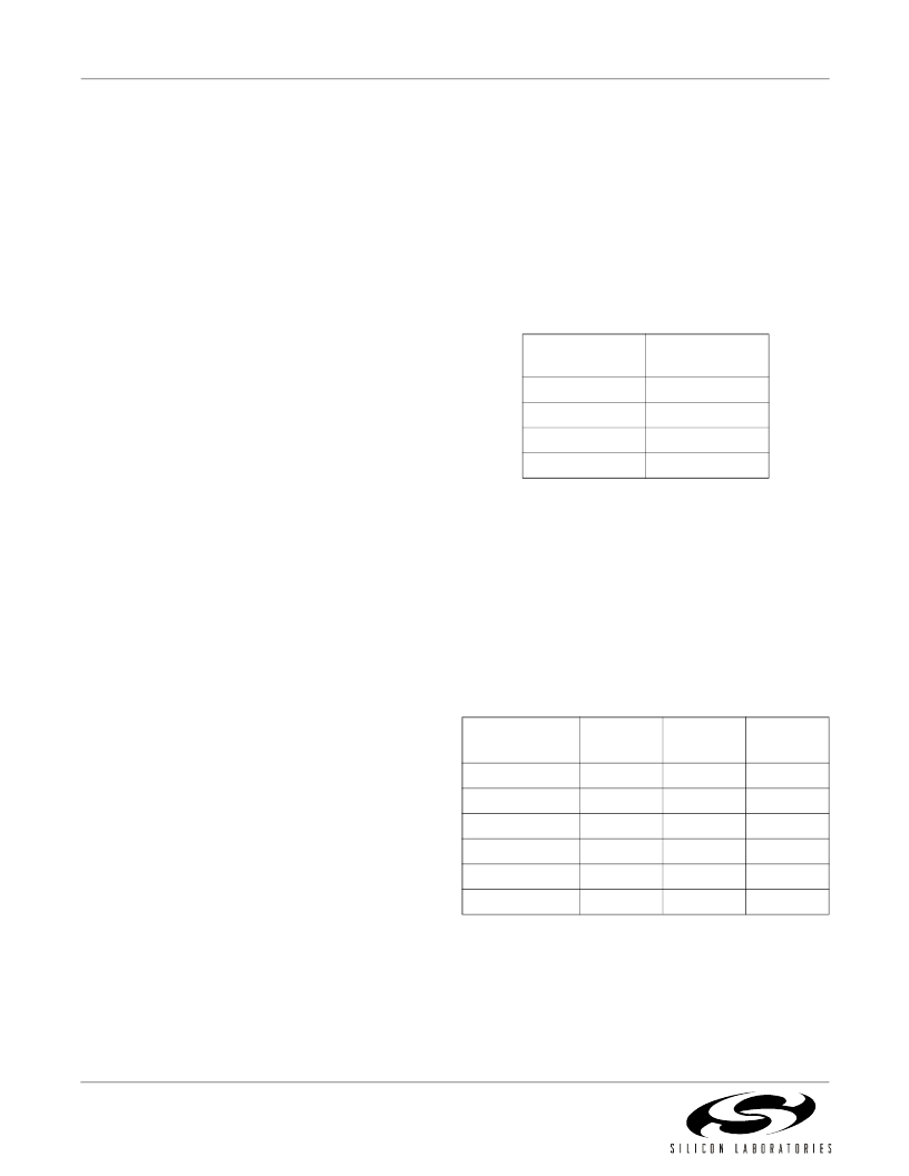
Table 8. Gain Values (Register 1)
K
P
Bits
Relative P.D.
Gain
00
1
01
1/2
10
1/4
11
1/8
Table 9. Optimal K
P
Settings
N
RF1
K
P1
<1:0>
00
RF2
K
P2
<3:2>
00
IF
K
PI
<5:4>
00
≤
2047
2048 to 4095
00
00
01
4096 to 8191
00
01
10
8192 to 16383
01
10
11
16384 to 32767
≥
32768
10
11
11
11
11
11
相關(guān)PDF資料 |
PDF描述 |
|---|---|
| Si4133-BT | DUAL-BAND RF SYNTHESIZER WITH INTEGRATED VCOS FOR WIRELESS COMMUNICATIONS |
| SI4136 | ISM RF SYNTHESIZER WITH INTEGRATED VCOS |
| SI4136-BT | ISM RF SYNTHESIZER WITH INTEGRATED VCOS |
| SI5010 | OC-12/3, STM-4/1 SONET/SDH CLOCK AND DATA RECOVERY IC |
| Si5010-BM | OC-12/3, STM-4/1 SONET/SDH CLOCK AND DATA RECOVERY IC |
相關(guān)代理商/技術(shù)參數(shù) |
參數(shù)描述 |
|---|---|
| SI4133-BMR | 功能描述:射頻無線雜項(xiàng) General Purpose RoHS:否 制造商:Texas Instruments 工作頻率:112 kHz to 205 kHz 電源電壓-最大:3.6 V 電源電壓-最小:3 V 電源電流:8 mA 最大功率耗散: 工作溫度范圍:- 40 C to + 110 C 封裝 / 箱體:VQFN-48 封裝:Reel |
| SI4133-BT | 功能描述:射頻無線雜項(xiàng) USE 634-SI4133-D-GT FOR NEW DESIGNS RoHS:否 制造商:Texas Instruments 工作頻率:112 kHz to 205 kHz 電源電壓-最大:3.6 V 電源電壓-最小:3 V 電源電流:8 mA 最大功率耗散: 工作溫度范圍:- 40 C to + 110 C 封裝 / 箱體:VQFN-48 封裝:Reel |
| SI4133DGM | 制造商:SILICONIX 功能描述:Pb Free 制造商:Silicon Laboratories Inc 功能描述: |
| SI4133-D-GM | 功能描述:鎖相環(huán) - PLL DUAL-BAND RF MLP-28 RoHS:否 制造商:Silicon Labs 類型:PLL Clock Multiplier 電路數(shù)量:1 最大輸入頻率:710 MHz 最小輸入頻率:0.002 MHz 輸出頻率范圍:0.002 MHz to 808 MHz 電源電壓-最大:3.63 V 電源電壓-最小:1.71 V 最大工作溫度:+ 85 C 最小工作溫度:- 40 C 封裝 / 箱體:QFN-36 封裝:Tray |
| SI4133-D-GMR | 功能描述:射頻無線雜項(xiàng) Dual-Band RF Synthesizer RoHS:否 制造商:Texas Instruments 工作頻率:112 kHz to 205 kHz 電源電壓-最大:3.6 V 電源電壓-最小:3 V 電源電流:8 mA 最大功率耗散: 工作溫度范圍:- 40 C to + 110 C 封裝 / 箱體:VQFN-48 封裝:Reel |
發(fā)布緊急采購,3分鐘左右您將得到回復(fù)。