- 您現(xiàn)在的位置:買(mǎi)賣(mài)IC網(wǎng) > PDF目錄374786 > SHF-0589 (Electronic Theatre Controls, Inc.) 0.05-3 GHz, 2 Watt GaAs HFET PDF資料下載
參數(shù)資料
| 型號(hào): | SHF-0589 |
| 廠商: | Electronic Theatre Controls, Inc. |
| 英文描述: | 0.05-3 GHz, 2 Watt GaAs HFET |
| 中文描述: | 0.05-3千兆赫,2瓦特砷化鎵異質(zhì)結(jié)場(chǎng)效應(yīng)晶體管 |
| 文件頁(yè)數(shù): | 2/4頁(yè) |
| 文件大小: | 195K |
| 代理商: | SHF-0589 |
SHF-0589 2 Watt HFET
2
EDS-101242 Rev F
522 Almanor Ave., Sunnyvale, CA 94085
Phone: (800) SMI-MMIC
http://www.sirenza.com
Absolute Maximum Ratings
r
e
m
a
r
a
P
l
o
b
m
y
e
u
V
t
n
U
n
t
e
I
0
4
6
A
m
e
d
w
r
t
e
I
8
A
m
t
e
e
e
s
v
e
I
8
A
m
e
c
o
-
e
g
a
V
V
0
V
e
c
o
-
e
g
a
V
V
0
>
r
5
V
r
w
o
P
t
p
n
P
I
0
0
8
m
g
n
p
d
a
e
L
e
p
m
e
L
h
p
a
e
e
°
e
g
n
a
e
p
m
e
e
g
a
r
1
+
o
0
4
5
6
°
n
o
p
s
r
w
o
P
P
h
p
a
e
e
e
p
m
e
l
n
n
a
h
J
5
6
1
°
e
e
e
s
u
a
c
e
u
v
c
y
a
e
m
s
h
n
p
o
m
i
e
s
o
p
m
u
m
e
o
h
u
o
u
a
m
e
h
e
n
o
y
o
d
n
c
a
d
n
e
x
e
.
e
o
y
e
a
t
n
g
a
p
b
e
r
t
u
m
o
e
a
c
e
.
g
t
d
s
a
d
t
e
n
d
n
a
e
n
d
e
e
n
o
p
m
r
p
a
v
p
s
d
g
s
i
n
a
m
e
c
e
h
a
g
s
e
c
n
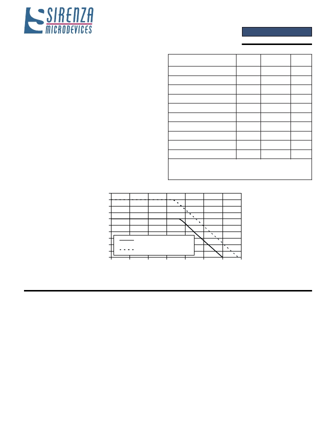
MTTF is inversely proportional to the device junction
temperature. For junction temperature and MTTF
considerations the bias condition should also
satisfy the following expression:
P
DC
< (T
J
- T
L
) / R
TH
where:
P
DC
= I
* V
(W)
J
= Junction Temperature (°C)
L
= Lead Temperature (pin 4) (°C)
TH
= Thermal Resistance (°C/W)
1. The SHF-0x89 is a depletion mode FET and requires a negative gate voltage. Normal pinchoff variation from part-to-
part precludes the use of a fixed gate voltage for all devices. Active bias circuitry or manual gate bias alignment is
recommended to maintain acceptable performance (RF and thermal).
2. Active bias circuitry is strongly recommended for class A operation (backoff >6dB).
3. For large signal operation (< 6dB backoff) class AB operation is required to maximize the FET’s performance.
Passive gate bias circuitry is generally required to achieve pure class AB performance. This is generally accomplished
using a voltage divider with temperature compensation. Per item 1 above the gate voltage should be aligned for each
device to eliminate the effects of pinchoff process variation.
4. Choose the operating voltage based on the amount of backoff. For large signal operation the drain-source voltage
should be increased to 8V to maximize P1dB. For small signal operation OIP3 may be improved by reducing the voltage
and increasing the current. The recommended application circuit should be re-optimized if the recommended 7V bias
condition is not used. Make sure the quiescent bias condition does not exceed the recommended power dissipation
limit (shown on page 1).
Design Considerations and Trade-offs
0.0
0.5
1.0
1.5
2.0
2.5
3.0
3.5
4.0
4.5
5.0
-40
-10
20
Lead Temperature (C)
50
80
110
140
170
Operational (Tj<140C)
ABS MAX (Tj<165C)
Power Derating Curve
NOTRECOMMENDEDFORNEWDESGN
相關(guān)PDF資料 |
PDF描述 |
|---|---|
| SHF5110 | IR-Receiver for Remote Control Systems |
| SHF5111 | IR-Receiver for Remote Control Systems |
| SHM-12 | Ultra-Fast, 12-Bit Linear Monolithic Sample-Hold Amplifiers |
| SHM-12L | Ultra-Fast, 12-Bit Linear Monolithic Sample-Hold Amplifiers |
| SHM-12LM | Ultra-Fast, 12-Bit Linear Monolithic Sample-Hold Amplifiers |
相關(guān)代理商/技術(shù)參數(shù) |
參數(shù)描述 |
|---|---|
| SHF-102-01-F-D-TH | 制造商:Samtec Inc 功能描述:.050 X .050 SHROUDED TERMINAL STRIP - Bulk |
| SHF-102-01-L-D-SM | 制造商:Samtec Inc 功能描述:.050 X .050 SHROUDED TERMINAL STRIP - Bulk |
| SHF-102-01-L-D-TH | 制造商:Samtec Inc 功能描述:CONNECTOR |
| SHF-103-01-F-D-SM-K-TR | 制造商:Samtec Inc 功能描述:.050 X .050 SHROUDED TERMINAL STRIP - Tape and Reel |
| SHF-103-01-F-D-TH | 制造商:Samtec Inc 功能描述:.050 X .050 SHROUDED TERMINAL STRIP - Bulk |
發(fā)布緊急采購(gòu),3分鐘左右您將得到回復(fù)。