- 您現(xiàn)在的位置:買賣IC網(wǎng) > PDF目錄374732 > SC483 (Semtech Corporation) Dual Synchronous Buck Pseudo Fixed Frequency Power Supply Controller PDF資料下載
參數(shù)資料
| 型號: | SC483 |
| 廠商: | Semtech Corporation |
| 英文描述: | Dual Synchronous Buck Pseudo Fixed Frequency Power Supply Controller |
| 中文描述: | 雙同步降壓偽固定頻率電源控制器 |
| 文件頁數(shù): | 21/27頁 |
| 文件大?。?/td> | 478K |
| 代理商: | SC483 |
第1頁第2頁第3頁第4頁第5頁第6頁第7頁第8頁第9頁第10頁第11頁第12頁第13頁第14頁第15頁第16頁第17頁第18頁第19頁第20頁當(dāng)前第21頁第22頁第23頁第24頁第25頁第26頁第27頁
21
2005 Semtech Corp.
www.semtech.com
SC483
POWER MANAGEMENT
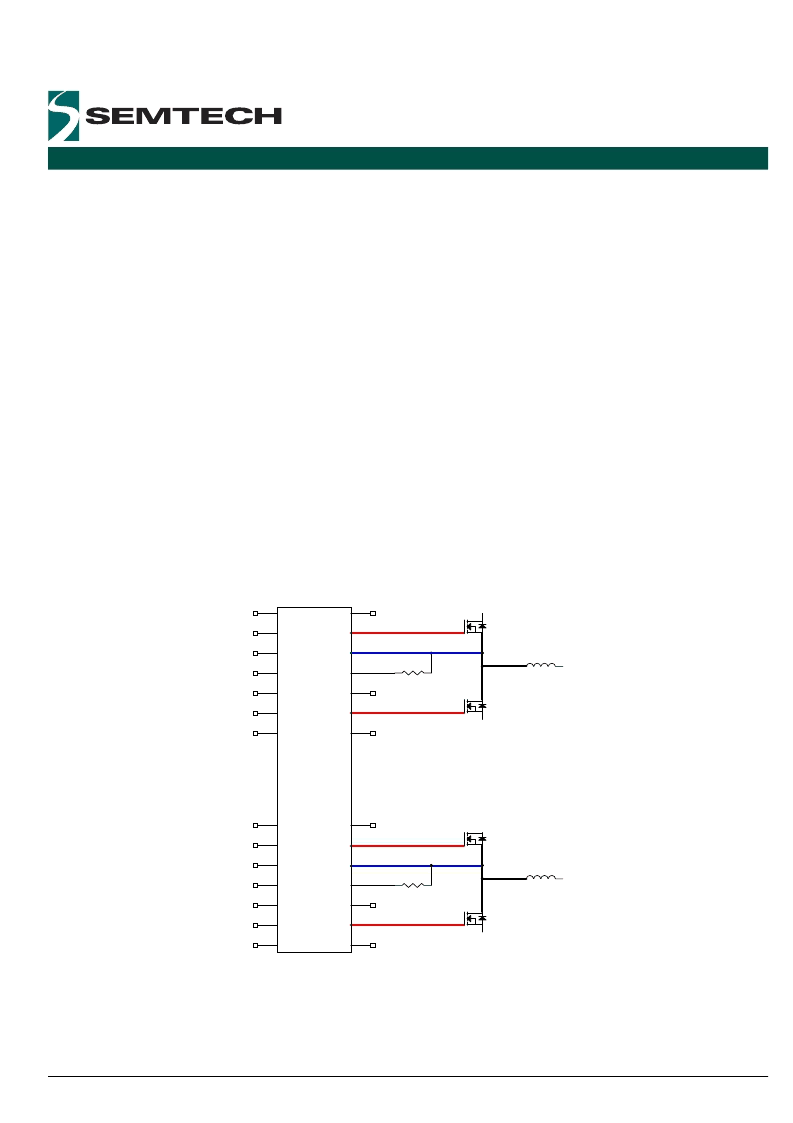
Key points for the power section:
1) there should be a very small input loop, well decoupled.
2) the phase node should be a large copper pour, but compact since this is the noisiest node.
3) input power ground and output power ground should not connect directly, but through the ground planes instead.
4) The two outputs should not share their input capacitors, and these should have separate PWR_SRC and PGND
(component-side) copper pours.
5) The two output inductors should not be placed adjacent to each other to avoid crosstalk.
6) Notice in Figure 13 placement of 0
resistor at the bottom of the output capacitor to connect to VSSA1/2 for
each output.
Connecting the control and power sections should be accomplished as follows (see Figure 14 below):
1) Route VSSA1/2 and their related feedback traces as differential pairs routed in a “quiet” layer away from noise
sources.
2) Route DL, DH and LX (low side FET gate drive, high side FET gate drive and phase node) to chip using wide traces
with multiple vias if using more than one layer. These connections to be as short as possible for loop minimization,
with a length to width ratio less than 20:1 to minimize impedance. DL is the most critical gate drive, with power
ground as its return path. LX is the noisiest node in the circuit, switching between PWR_SRC and ground at high
frequencies, thus should be kept as short as practical. DH has LX as its return path.
3) BST is also a noisy node and should be kept as short as possible.
4) Connect PGND pins on the chip directly to the VDDP decoupling capacitor and then drop vias directly to the
ground plane.
5) Locate the current limit sense resistors between the LX and ILIM pins at the device.
0402
EN/PSV1
22
TON1
23
VOUT1
24
VCCA1
25
FB1
26
PGD1
27
VSSA1
28
PGND1
1
DL1
2
VDDP1
3
ILIM1
4
LX1
5
DH1
6
BST1
7
EN/PSV2
8
TON2
9
VOUT2
10
VCCA2
11
FB2
12
PGD2
13
VSSA2
14
PGND2
15
DL2
16
VDDP2
17
ILIM2
18
LX2
19
DH2
20
BST2
21
U1
SC483
Q2
Q1
R5
L1
0402
Q3
IRF7811AV
Q4
FDS6676S
R10 7k87
L2
2u2
Figure 14: Connecting Control and Power Sections
Phase nodes (black) to be copper islands (preferred) or wide copper traces. Gate drive traces (red) and phase node
traces (blue) to be wide copper traces (L:W < 20:1) and as short as possible, with DL the most critical.
相關(guān)PDF資料 |
PDF描述 |
|---|---|
| SC483ITSTRT | Dual Synchronous Buck Pseudo Fixed Frequency Power Supply Controller |
| SC486 | Complete DDR1/2/3 Memory Power Supply |
| SC486EVB | Complete DDR1/2/3 Memory Power Supply |
| SC486IMLTRT | Complete DDR1/2/3 Memory Power Supply |
| SC488 | Complete DDR1/2/3 Memory Power Supply |
相關(guān)代理商/技術(shù)參數(shù) |
參數(shù)描述 |
|---|---|
| SC483ITSTRT | 制造商:SEMTECH 制造商全稱:Semtech Corporation 功能描述:Dual Synchronous Buck Pseudo Fixed Frequency Power Supply Controller |
| SC486 | 制造商:SEMTECH 制造商全稱:Semtech Corporation 功能描述:Complete DDR1/2/3 Memory Power Supply |
| SC486EVB | 制造商:SEMTECH 制造商全稱:Semtech Corporation 功能描述:Complete DDR1/2/3 Memory Power Supply |
| SC486IML.TRTCUT | 制造商:Semtech Corporation 功能描述: |
| SC486IMLTRT | 制造商:Semtech Corporation 功能描述:Power Supply 24-Pin MLPQ EP T/R 制造商:Semtech Corporation 功能描述:POWER SUPPLY DDR 1 2 3 MEM SMD |
發(fā)布緊急采購,3分鐘左右您將得到回復(fù)。