- 您現(xiàn)在的位置:買賣IC網(wǎng) > PDF目錄296691 > NJG1515AVB2 RF/MICROWAVE TRANSFER SWITCH PDF資料下載
參數(shù)資料
| 型號: | NJG1515AVB2 |
| 元件分類: | 開關(guān) |
| 英文描述: | RF/MICROWAVE TRANSFER SWITCH |
| 封裝: | SSOP-20 |
| 文件頁數(shù): | 16/18頁 |
| 文件大小: | 549K |
| 代理商: | NJG1515AVB2 |
NJG1515AVB2
- 7 -
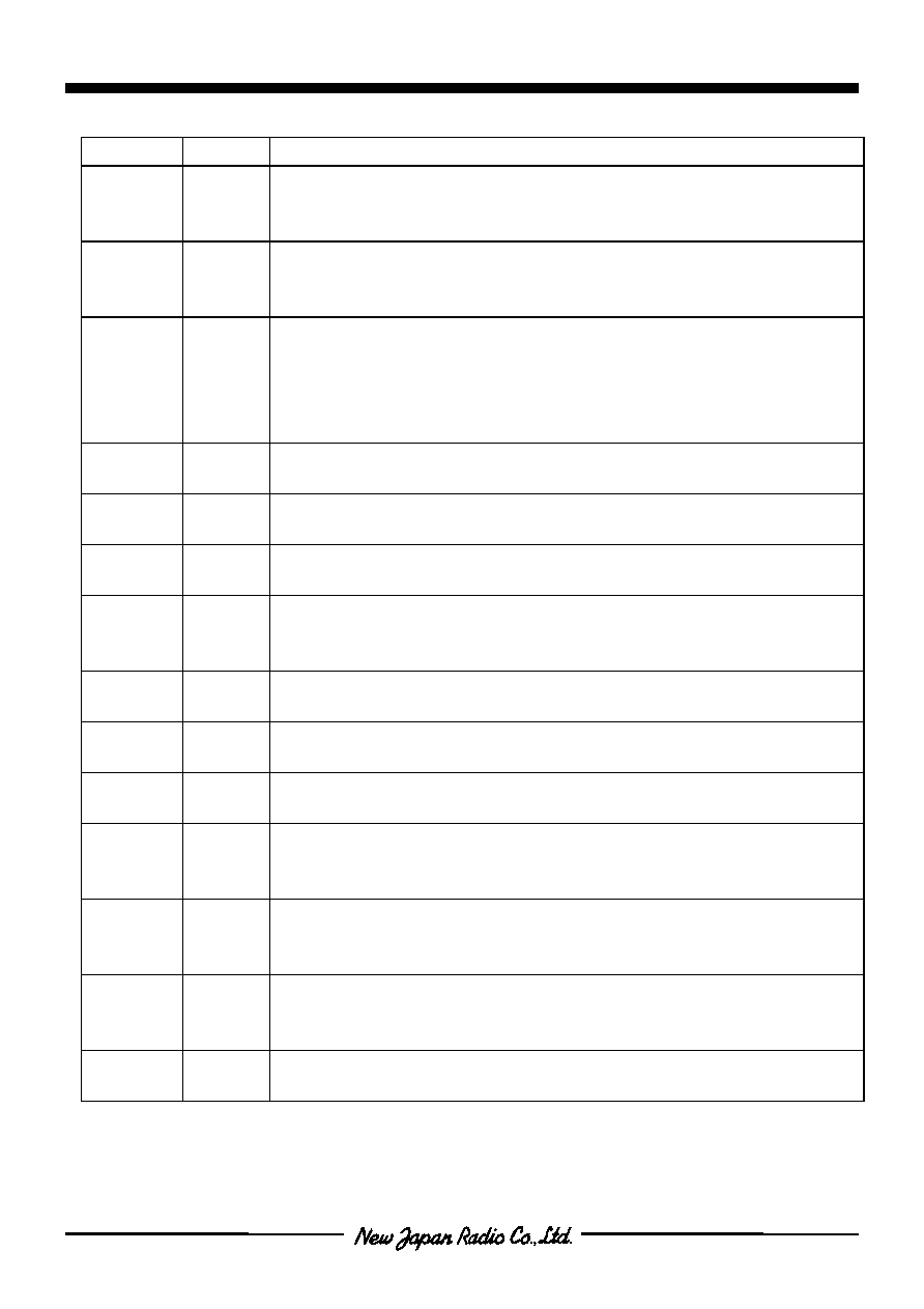
nTERMINAL INFORMATION
PIN NO.
SYMBOL
DESCRIPTIONS
1
CTL2
High-impedance C-MOS input terminal. This terminal is set to High-Level by
2V~VDD, and Low-Level by +0.6V~0V. In case of open or unstable level,
connect this terminal by 100K
resistor with GND terminal or V
DD terminal.
2
CTL3
High-impedance C-MOS input terminal. This terminal is set to High-Level by
2V~VDD, and Low-Level by +0.6V~0V. In case of open or unstable level,
connect this terminal by 100K
resistor with GND terminal or V
DD terminal.
3
VSS
Negative voltage supply terminal. The negative voltage (-3.5~-2.0V) have to
be supplied on transmitting. Otherwise negative voltage of -2.5~0V can be
used or this terminal can be stayed open, because internal level of this
terminal is automatically set to GND level on receiving. The bypass capacitor
have to be connected with GND terminal for excellent RF performance.
4
EXT2
RF receiving port. An external capacitor of 56pF~100pF is required to block
DC voltage (VDD).
6
EXT1
RF transmitting/receiving port. An external capacitor of 56pF~100pF is
required to block DC voltage (VDD).
8
TX
RF transmitting port. An external capacitor of 56pF~100pF is required to
block DC voltage (VDD).
10
TER2
ANT1 termination port. The influence of ANT1 port to ANT2 port is
suppressed by terminating this port by an appropriate termination. An
external capacitor (5pF) is required to block DC voltage (VDD).
11
ANT1
RF transmitting/receiving port. An external capacitor of 56pF~100pF is
required to block DC voltage (VDD).
13
RX
RF receiving port. An external capacitor of 56pF~100pF is required to block
DC voltage (VDD).
15
ANT2
RF receiving port. An external capacitor of 56pF~100pF is required to block
DC voltage (VDD).
17
TER1
ANT2 termination port. The influence of ANT2 port to ANT1 port is
suppressed by terminating this port with appropriate termination. An external
capacitor (5pF) is required to block DC voltage (VDD).
19
VDD
Positive voltage supply terminal. The positive voltage (2.7~5.0V) have to be
supplied. The bypass capacitor have to be connected with GND terminal for
excellent RF performance.
20
CTL1
High-impedance C-MOS input terminal. This terminal is set to High-Level by
2V~VDD, and Low-Level by +0.6~0V. In case of open or unstable level,
connect this terminal by 100k
resistor with GND terminal or V
DD terminal.
5,7,9,12,
14,16,18
GND
Ground terminal. Please connect this terminal with ground plane as close as
possible for excellent RF performance.
相關(guān)PDF資料 |
PDF描述 |
|---|---|
| NJG1667MD7 | 1000 MHz - 2500 MHz RF/MICROWAVE SGL POLE FIVE THROW SWITCH, 0.8 dB INSERTION LOSS |
| NJU6319DC | 6.25 MHz, OTHER CLOCK GENERATOR, UUC6 |
| NJU6338BE | 17.5 MHz, OTHER CLOCK GENERATOR, PDSO8 |
| NJU6338KE-(T2) | 12.5 MHz, OTHER CLOCK GENERATOR, PDSO8 |
| NJU6338BE-(TE2) | 17.5 MHz, OTHER CLOCK GENERATOR, PDSO8 |
相關(guān)代理商/技術(shù)參數(shù) |
參數(shù)描述 |
|---|---|
| NJG1515AVB2-C1 | 制造商:NJRC 制造商全稱:New Japan Radio 功能描述:TDMA ANTENNA SWITCH GaAs MMIC |
| NJG1515AVB2-C10 | 制造商:NJRC 制造商全稱:New Japan Radio 功能描述:TDMA ANTENNA SWITCH GaAs MMIC |
| NJG1515AVB2-C2 | 制造商:NJRC 制造商全稱:New Japan Radio 功能描述:TDMA ANTENNA SWITCH GaAs MMIC |
| NJG1515AVB2-C3 | 制造商:NJRC 制造商全稱:New Japan Radio 功能描述:TDMA ANTENNA SWITCH GaAs MMIC |
| NJG1515AVB2-C4 | 制造商:NJRC 制造商全稱:New Japan Radio 功能描述:TDMA ANTENNA SWITCH GaAs MMIC |
發(fā)布緊急采購,3分鐘左右您將得到回復(fù)。