- 您現(xiàn)在的位置:買賣IC網(wǎng) > PDF目錄359234 > MT9072AV (ZARLINK SEMICONDUCTOR INC) Ultraframer DS3/E3/DS2/E2/DS1/E1/DS0 PDF資料下載
參數(shù)資料
| 型號(hào): | MT9072AV |
| 廠商: | ZARLINK SEMICONDUCTOR INC |
| 元件分類: | 數(shù)字傳輸電路 |
| 英文描述: | Ultraframer DS3/E3/DS2/E2/DS1/E1/DS0 |
| 中文描述: | DATACOM, FRAMER, PBGA220 |
| 封裝: | 17 X 17 MM, 1.30 MM HEIGHT, MO-192, LBGA-220 |
| 文件頁(yè)數(shù): | 24/275頁(yè) |
| 文件大小: | 3738K |
| 代理商: | MT9072AV |
第1頁(yè)第2頁(yè)第3頁(yè)第4頁(yè)第5頁(yè)第6頁(yè)第7頁(yè)第8頁(yè)第9頁(yè)第10頁(yè)第11頁(yè)第12頁(yè)第13頁(yè)第14頁(yè)第15頁(yè)第16頁(yè)第17頁(yè)第18頁(yè)第19頁(yè)第20頁(yè)第21頁(yè)第22頁(yè)第23頁(yè)當(dāng)前第24頁(yè)第25頁(yè)第26頁(yè)第27頁(yè)第28頁(yè)第29頁(yè)第30頁(yè)第31頁(yè)第32頁(yè)第33頁(yè)第34頁(yè)第35頁(yè)第36頁(yè)第37頁(yè)第38頁(yè)第39頁(yè)第40頁(yè)第41頁(yè)第42頁(yè)第43頁(yè)第44頁(yè)第45頁(yè)第46頁(yè)第47頁(yè)第48頁(yè)第49頁(yè)第50頁(yè)第51頁(yè)第52頁(yè)第53頁(yè)第54頁(yè)第55頁(yè)第56頁(yè)第57頁(yè)第58頁(yè)第59頁(yè)第60頁(yè)第61頁(yè)第62頁(yè)第63頁(yè)第64頁(yè)第65頁(yè)第66頁(yè)第67頁(yè)第68頁(yè)第69頁(yè)第70頁(yè)第71頁(yè)第72頁(yè)第73頁(yè)第74頁(yè)第75頁(yè)第76頁(yè)第77頁(yè)第78頁(yè)第79頁(yè)第80頁(yè)第81頁(yè)第82頁(yè)第83頁(yè)第84頁(yè)第85頁(yè)第86頁(yè)第87頁(yè)第88頁(yè)第89頁(yè)第90頁(yè)第91頁(yè)第92頁(yè)第93頁(yè)第94頁(yè)第95頁(yè)第96頁(yè)第97頁(yè)第98頁(yè)第99頁(yè)第100頁(yè)第101頁(yè)第102頁(yè)第103頁(yè)第104頁(yè)第105頁(yè)第106頁(yè)第107頁(yè)第108頁(yè)第109頁(yè)第110頁(yè)第111頁(yè)第112頁(yè)第113頁(yè)第114頁(yè)第115頁(yè)第116頁(yè)第117頁(yè)第118頁(yè)第119頁(yè)第120頁(yè)第121頁(yè)第122頁(yè)第123頁(yè)第124頁(yè)第125頁(yè)第126頁(yè)第127頁(yè)第128頁(yè)第129頁(yè)第130頁(yè)第131頁(yè)第132頁(yè)第133頁(yè)第134頁(yè)第135頁(yè)第136頁(yè)第137頁(yè)第138頁(yè)第139頁(yè)第140頁(yè)第141頁(yè)第142頁(yè)第143頁(yè)第144頁(yè)第145頁(yè)第146頁(yè)第147頁(yè)第148頁(yè)第149頁(yè)第150頁(yè)第151頁(yè)第152頁(yè)第153頁(yè)第154頁(yè)第155頁(yè)第156頁(yè)第157頁(yè)第158頁(yè)第159頁(yè)第160頁(yè)第161頁(yè)第162頁(yè)第163頁(yè)第164頁(yè)第165頁(yè)第166頁(yè)第167頁(yè)第168頁(yè)第169頁(yè)第170頁(yè)第171頁(yè)第172頁(yè)第173頁(yè)第174頁(yè)第175頁(yè)第176頁(yè)第177頁(yè)第178頁(yè)第179頁(yè)第180頁(yè)第181頁(yè)第182頁(yè)第183頁(yè)第184頁(yè)第185頁(yè)第186頁(yè)第187頁(yè)第188頁(yè)第189頁(yè)第190頁(yè)第191頁(yè)第192頁(yè)第193頁(yè)第194頁(yè)第195頁(yè)第196頁(yè)第197頁(yè)第198頁(yè)第199頁(yè)第200頁(yè)第201頁(yè)第202頁(yè)第203頁(yè)第204頁(yè)第205頁(yè)第206頁(yè)第207頁(yè)第208頁(yè)第209頁(yè)第210頁(yè)第211頁(yè)第212頁(yè)第213頁(yè)第214頁(yè)第215頁(yè)第216頁(yè)第217頁(yè)第218頁(yè)第219頁(yè)第220頁(yè)第221頁(yè)第222頁(yè)第223頁(yè)第224頁(yè)第225頁(yè)第226頁(yè)第227頁(yè)第228頁(yè)第229頁(yè)第230頁(yè)第231頁(yè)第232頁(yè)第233頁(yè)第234頁(yè)第235頁(yè)第236頁(yè)第237頁(yè)第238頁(yè)第239頁(yè)第240頁(yè)第241頁(yè)第242頁(yè)第243頁(yè)第244頁(yè)第245頁(yè)第246頁(yè)第247頁(yè)第248頁(yè)第249頁(yè)第250頁(yè)第251頁(yè)第252頁(yè)第253頁(yè)第254頁(yè)第255頁(yè)第256頁(yè)第257頁(yè)第258頁(yè)第259頁(yè)第260頁(yè)第261頁(yè)第262頁(yè)第263頁(yè)第264頁(yè)第265頁(yè)第266頁(yè)第267頁(yè)第268頁(yè)第269頁(yè)第270頁(yè)第271頁(yè)第272頁(yè)第273頁(yè)第274頁(yè)第275頁(yè)
MT9072
Data Sheet
24
Zarlink Semiconductor Inc.
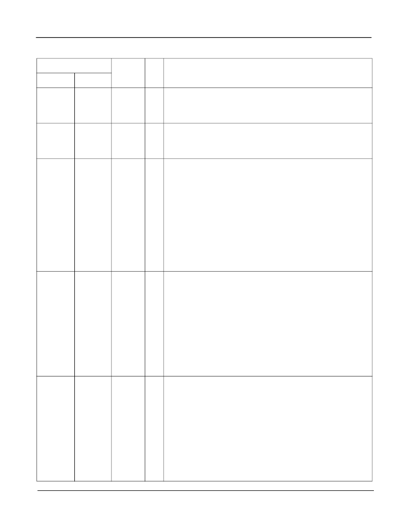
Pin Description
Pin #
Name
Type
Description (see Notes 1 to 7)
LQFP
LBGA
1,21,41,61,
81,101,121,
141,161,
179
E7,E8,E9,
E10,E11,
M7,M8,M9,
M10,M11
V
SS
P
Ground.
0V
DC
.
2,22,42,62,
82,102,122,
142,162,18
0
G5,H5,J5,
K5,L5,G12,
H12J12,K1
2,L12
V
DD
P
Supply Voltage.
+3.3 V
DC
nominal.
3
23
43
63
83
103
123
143
D1
H3
N1
N7
P9
R15
K13
F15
RPOS[0]
RPOS[1]
RPOS[2]
RPOS[3]
RPOS[4]
RPOS[5]
RPOS[6]
RPOS[7]
I
Receive Positive.
This pin is an input for the receive side of the
framer; it typically interfaces to an LIU. If used by itself it can accept
single rail NRZ (Non Return to Zero) data. If RPOS is used in
conjunction with RNEG it can accept dual rail NRZ data or dual rail RZ
(Return to Zero) data. The clock at the EXCLi pin is used to clock data
into the RPOS pin. Pins RPOS[0-7] are used for Framers[0-7]
respectively.
In T1 mode, transmit line codes are selected with control bits:
RZCS1-0, RXB8ZS, RZNRZ and UNIBI (Address Y01). T1 mode is
selected if the T1E0 bit (Address 900) is 1.
In E1 mode, line codes are selected with control bits: COD0-1 and
RHDB3 at (Address Y02). E1 mode is selected if the T1E0 bit
(Address 900) is 0.
4
24
44
64
84
104
124
144
D2
H4
N2
N8
P10
R16
K14
F16
RNEG[0]
RNEG[1]
RNEG[2]
RNEG[3]
RNEG[4]
RNEG[5]
RNEG[6]
RNEG[7]
I
Receive Negative.
This pin is an input for the receive side of the
framer; it typically interfaces to an LIU. RNEG is used in conjunction
with RPOS to accept dual rail NRZ (Non Return to Zero) data or dual
rail RZ (Return to Zero) data. The clock at the EXCLi pin is used to
clock data into the RNEG pin. Pins RNEG[0-7] are used for
Framers[0-7] respectively.
In T1 mode, receive line codes are selected with control bits:
RZCS1-0, RXB8ZS, RZNRZ and UNIBI at (Address Y01). T1 mode is
selected if the T1E0 bit (Address 900) is 1.
In E1 mode, line codes are selected with control bits: COD0-1 and
RHDB3 at (Address Y02). E1 mode is selected if the T1E0 bit
(Address 900) is 0.
5
25
45
65
85
105
125
145
D3
J1
N3
P5
P11
P13
K15
E13
EXCLi(0)
EXCLi(1)
EXCLi(2)
EXCLi(3)
EXCLi(4)
EXCLi(5)
EXCLi(6)
EXCLi(7)
I
1.544/2.048 MHz Extracted Clock.
The rising edge of the clock
applied at this input is used to clock RZ data into the receive side of
the framer on pins RPOS and RNEG. If RPOS/RNEG are configured
for NRZ input then either a rising or falling edge on the EXCLi clock
can be selected to clock RPOS/RNEG data. Pins EXCLi[0-7] are used
for Framers[0-7] respectively.
In T1 mode, this pin accepts a 1.544 MHz extracted clock. An active
rising or falling edge is selected with the CLKE bit (Address Y01). See
Figure 53.
In E1 mode, this pin accepts a 2.048 MHz extracted clock. An active
rising or falling edge is selected with the CLKE bit (Address Y02). See
Figure 73.
相關(guān)PDF資料 |
PDF描述 |
|---|---|
| MT90820 | Large Digital Switch |
| MT90820AL | Large Digital Switch |
| MT90820AL1 | Large Digital Switch |
| MT90823AL1 | 3V Large Digital Switch |
| MT90823 | 3V Large Digital Switch |
相關(guān)代理商/技術(shù)參數(shù) |
參數(shù)描述 |
|---|---|
| MT9072AV2 | 制造商:Microsemi Corporation 功能描述:FRAMER E1/J1/T1 3.3V 220BGA - Trays 制造商:Zarlink Semiconductor Inc 功能描述:FRAMER E1/J1/T1 3.3V 220BGA - Trays |
| MT90732 | 制造商:MITEL 制造商全稱:Mitel Networks Corporation 功能描述:CMOS E2/E3 Framer (E2/E3F) |
| MT90732AP | 制造商:MITEL 制造商全稱:Mitel Networks Corporation 功能描述:CMOS E2/E3 Framer (E2/E3F) |
| MT90733 | 制造商:MITEL 制造商全稱:Mitel Networks Corporation 功能描述:CMOS DS3 Framer (DS3F) |
| MT90733AP | 制造商:MITEL 制造商全稱:Mitel Networks Corporation 功能描述:CMOS DS3 Framer (DS3F) |
發(fā)布緊急采購(gòu),3分鐘左右您將得到回復(fù)。