- 您現(xiàn)在的位置:買(mǎi)賣(mài)IC網(wǎng) > PDF目錄359234 > MT8986AP (Mitel Networks Corporation) CMOS ST-BUS⑩ FAMILY Multiple Rate Digital Switch PDF資料下載
參數(shù)資料
| 型號(hào): | MT8986AP |
| 廠商: | Mitel Networks Corporation |
| 英文描述: | CMOS ST-BUS⑩ FAMILY Multiple Rate Digital Switch |
| 中文描述: | 意法半導(dǎo)體的CMOS總線(xiàn)⑩家庭多速率數(shù)字開(kāi)關(guān) |
| 文件頁(yè)數(shù): | 21/46頁(yè) |
| 文件大?。?/td> | 765K |
| 代理商: | MT8986AP |
第1頁(yè)第2頁(yè)第3頁(yè)第4頁(yè)第5頁(yè)第6頁(yè)第7頁(yè)第8頁(yè)第9頁(yè)第10頁(yè)第11頁(yè)第12頁(yè)第13頁(yè)第14頁(yè)第15頁(yè)第16頁(yè)第17頁(yè)第18頁(yè)第19頁(yè)第20頁(yè)當(dāng)前第21頁(yè)第22頁(yè)第23頁(yè)第24頁(yè)第25頁(yè)第26頁(yè)第27頁(yè)第28頁(yè)第29頁(yè)第30頁(yè)第31頁(yè)第32頁(yè)第33頁(yè)第34頁(yè)第35頁(yè)第36頁(yè)第37頁(yè)第38頁(yè)第39頁(yè)第40頁(yè)第41頁(yè)第42頁(yè)第43頁(yè)第44頁(yè)第45頁(yè)第46頁(yè)
MT8986
Data Sheet
21
Zarlink Semiconductor Inc.
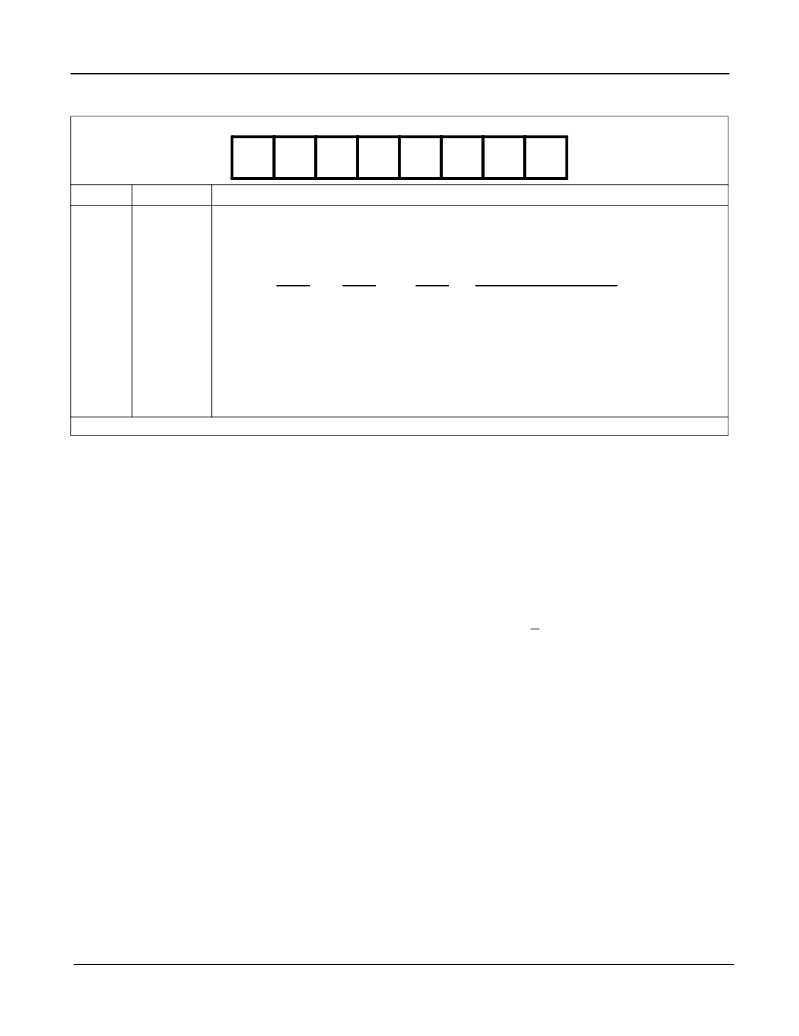
Frame Input Offset Register - Read/Write
Figure 8 - Frame Input Offset (FIO) Register
x=Don’t care
Applications
Switch Matrix Architectures
The MT8986 is an ideal device for designs of medium size switch matrix. For applications where voice and grouped
data channels are transported within the same frame, the voice samples have to be time interchanged with a
minimum delay while maintaining the integrity of grouped data. To guarantee the integrity of grouped data during
switching and to provide a minimum delay for voice connections, the MT8986 provides the per-channel selection
between variable and constant throughput delay. This can be selected by the V/C bit of the Connection Memory
High locations.
Different connectivities at different data rates can be built to accommodate Non-Blocking matrices of up to 512
channels while maintaining the per channel selection of the device's throughput delay. Some examples of such
Non-Blocking configurations are given in Figures 9 to 11.
For applications where voice and data samples are encoded into individual 64 kb/s time-slots on an 8 kHz frame
basis, the switch matrix can operate with time interchange procedures where only variable throughput delay is
guaranteed. For such applications, the MT8986 device allows cost effective implementations of Non-Blocking
matrices ranging up to 1024 channels. Figures 12 and 13 show the block diagram of implementations with Non-
Blocking capacities of 512 and 1024-channel, respectively.
BIT
7-5
NAME
OFB2-0
DESCRIPTION
Offset Bits 2-0
. These three bits define the time it takes the Serial Interface receiver to recognize
and store the first bit of the serial input streams; i.e., to start assuming a new internal frame. The
input frame offset can be selected to be up to 4 CK clock periods from the time when frame pulse
input signal is applied to the FR input.
OFB2
OFB1
OFB0
0
0
0
0
0
1
0
1
0
0
1
1
1
0
0
1
0
1
1
1
0
1
1
1
Number of Clock Periods
Normal Operation. No bit offsetting.
1
2
3
4
Reserved
Reserved
Reserved
If frame input offset operation is not required, this register should be cleared by the CPU during system initialization.
OFB2
OFB1
OFB0
X
X
X
X
X
7
6
5
4
3
2
1
0
相關(guān)PDF資料 |
PDF描述 |
|---|---|
| MT8D264G-6 | x64 Fast Page Mode DRAM Module |
| MT8D264G-6X | x64 EDO Page Mode DRAM Module |
| MT8D264G-7 | x64 Fast Page Mode DRAM Module |
| MT8D264G-7X | x64 EDO Page Mode DRAM Module |
| MT90401 | SONET/SDH System Synchronizer |
相關(guān)代理商/技術(shù)參數(shù) |
參數(shù)描述 |
|---|---|
| MT8986AP1 | 制造商:Microsemi Corporation 功能描述:SWIT FABRIC 256 X 256/512 X 256/128 X 128 131.072MBPS 5V 44P - Rail/Tube 制造商:MICROSEMI CONSUMER MEDICAL PRODUCT GROUP 功能描述:IC TDM/TSI SWITCH 512X256 44PLCC 制造商:Microsemi Corporation 功能描述:IC TDM/TSI SWITCH 512X256 44PLCC |
| MT8986APR | 制造商:TOSHIBA 制造商全稱(chēng):Toshiba Semiconductor 功能描述:CMOS ST-BUS Family Multiple Rate Digital Switch |
| MT8986APR1 | 制造商:Microsemi Corporation 功能描述:SWITES 44PLCC - Tape and Reel 制造商:MICROSEMI CONSUMER MEDICAL PRODUCT GROUP 功能描述:IC TDM/TSI SWITCH 512X256 44PLCC 制造商:Microsemi Corporation 功能描述:IC TDM/TSI SWITCH 512X256 44PLCC |
| MT8992BC | 制造商:MITEL 制造商全稱(chēng):Mitel Networks Corporation 功能描述:Digital Telephone with HDLC |
| MT8993BC | 制造商:MITEL 制造商全稱(chēng):Mitel Networks Corporation 功能描述:Digital Telephone with HDLC |
發(fā)布緊急采購(gòu),3分鐘左右您將得到回復(fù)。