- 您現(xiàn)在的位置:買賣IC網(wǎng) > PDF目錄359234 > MT8985APR1 (ZARLINK SEMICONDUCTOR INC) Enhanced Digital Switch PDF資料下載
參數(shù)資料
| 型號: | MT8985APR1 |
| 廠商: | ZARLINK SEMICONDUCTOR INC |
| 元件分類: | 路由/交換 |
| 英文描述: | Enhanced Digital Switch |
| 中文描述: | TELECOM, DIGITAL TIME SWITCH, PQCC44 |
| 封裝: | LEAD FREE, PLASTIC, MS-018AC, LCC-44 |
| 文件頁數(shù): | 6/26頁 |
| 文件大小: | 568K |
| 代理商: | MT8985APR1 |
第1頁第2頁第3頁第4頁第5頁當(dāng)前第6頁第7頁第8頁第9頁第10頁第11頁第12頁第13頁第14頁第15頁第16頁第17頁第18頁第19頁第20頁第21頁第22頁第23頁第24頁第25頁第26頁
MT8985
Data Sheet
6
Zarlink Semiconductor Inc.
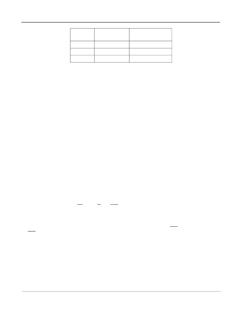
Table 1 - Channel Delay for the Variable Mode Delay
Constant Delay Mode
In this mode frame integrity is maintained in all switching configurations by making use of a multiple Data-Memory
buffer technique where input channels written in any of the buffers during frame N will be read out during frame
N+2. In the MT8985, the minimum throughput delay achievable in Constant Delay mode will be 32 time slots; for
example, when input time slot 32 (channel 31) is switched to output time slot 1 (channel 0). Likewise, the maximum
delay is achieved when the first time slot in a frame (channel 0) is switched to the last time slot in the frame
(channel 31), resulting in 94 time slots of delay.
To summarize, any input time slot from input frame N will be always switched to the destination time slot on output
frame N+2. In Constant Delay mode, the device throughput delay is calculated according to the following formula:
DELAY = [32 + (32 - IN) + (OUT - 1)];
(expressed in number of time slots)
Where:
IN is the number of the input time slot
(from 1 to 32).
OUT is the number of the output time slot
(from 1 to 32).
Microprocessor Port
The MT8985 microprocessor port has pin compatibility with Zarlink MT8980 Digital Switch device providing a non-
multiplexed bus architecture. The parallel port consists of an 8 bit parallel data bus (D0-D7), six address input lines
(A0-A5) and four control lines (CS, DS, R/W and DTA). This parallel microport allows the access to the Control
registers, Connection Memory High, Connection Memory Low and the Data Memory. All locations are read/written
except for the data memory which can be read only.
Accesses from the microport to the connection memory and the data memory are multiplexed with accesses from
the input and output TDM ports. This can cause variable Data Acknowledge delays (DTA). In the MT8985 device,
the DTA output provides a maximum acknowledgement delay of 800 ns for read/write operations in the Connection
Memory. However, for operations in the Data Memory (Message Mode), the maximum acknowledgement delay can
be 1220 ns.
Input
Channel
Output Channel
Throughput Delay
n
m=n, n+1 or n+2
m-n + 32 timeslots
n
m>n+2
m-n time slots
n
m<n
32-(n-m) time slots
相關(guān)PDF資料 |
PDF描述 |
|---|---|
| MT8985AP1 | Enhanced Digital Switch |
| MT8985 | CMOS ST-BUS⑩ FAMILY Enhanced Digital Switch |
| MT8985AE | CMOS ST-BUS⑩ FAMILY Enhanced Digital Switch |
| MT8985AL | CMOS ST-BUS⑩ FAMILY Enhanced Digital Switch |
| MT8985AP | CMOS ST-BUS⑩ FAMILY Enhanced Digital Switch |
相關(guān)代理商/技術(shù)參數(shù) |
參數(shù)描述 |
|---|---|
| MT8986 | 制造商:ZARLINK 制造商全稱:Zarlink Semiconductor Inc 功能描述:Multiple Rate Digital Switch |
| MT8986AC | 制造商:MITEL 制造商全稱:Mitel Networks Corporation 功能描述:CMOS ST-BUS⑩ FAMILY Multiple Rate Digital Switch |
| MT8986AE | 制造商:Microsemi Corporation 功能描述: |
| MT8986AE1 | 制造商:Microsemi Corporation 功能描述:PB FREE MULTIPLE RATE DIGITAL SWITCH 制造商:Microsemi Corporation 功能描述:SWIT FABRIC 256 X 256/512 X 256/128 X 128 131.072MBPS 5V 40P - Rail/Tube 制造商:MICROSEMI CONSUMER MEDICAL PRODUCT GROUP 功能描述:IC TDM/TSI SWITCH 512X256 40PDIP 制造商:Microsemi Corporation 功能描述:IC TDM/TSI SWITCH 512X256 40PDIP |
| MT8986AL | 制造商:Microsemi Corporation 功能描述:SWIT FABRIC 256 X 256/512 X 256/128 X 128 131.072MBPS 5V 44M - Trays 制造商:Zarlink Semiconductor Inc 功能描述:SWIT FABRIC 256 X 256/512 X 256/128 X 128 131.072MBPS 5V 44M - Trays |
發(fā)布緊急采購,3分鐘左右您將得到回復(fù)。