- 您現(xiàn)在的位置:買賣IC網(wǎng) > PDF目錄359232 > MT88E46AS (ZARLINK SEMICONDUCTOR INC) Bellcore Compliant Calling Number Identification Circuit PDF資料下載
參數(shù)資料
| 型號: | MT88E46AS |
| 廠商: | ZARLINK SEMICONDUCTOR INC |
| 元件分類: | 無繩電話/電話 |
| 英文描述: | Bellcore Compliant Calling Number Identification Circuit |
| 中文描述: | TELEPHONE CALLING NO IDENT CKT, PDSO20 |
| 封裝: | 0.300 INCH, MS-013AC, SOIC-20 |
| 文件頁數(shù): | 7/23頁 |
| 文件大?。?/td> | 522K |
| 代理商: | MT88E46AS |
Advance Information
MT88E46
7
Preliminary Off Hook Mode CAS
Detector Speech Immunity Performance
Since there is some randomness in speech immunity
testing, and because the telephone hybrid / speech
IC design will affect the result, the preliminary test
results in Tables 3 and 4 are provided to illustrate
typical performances only.
In Table 3 (talkoff results) column 3, the result was
obtained using pre-emphasized speech as both the
near end and far end speech sources. It is
pessimistic, as recognized in SR-TSV-002476,
because in reality the pre-emphasis originally
imparted on the far end speech by the far end CPE’s
microphone would have been equalized by the
subscriber loop, so that at the near end CPE Tip/
Ring terminals the far end speech would have no
pre-emphasis. Table 3 column 4 shows the result for
the same situation as column 3 except that pre-
emphasized speech was used only as the near end
speech source and normal speech was used as the
far end speech source, as allowed in SR-TSV-
002476.
In Table 3 column 5 and Table 4 column 4, the
MT88E46 performance with a telephone hybrid /
speech IC was simulated during testing by
attenuating the pre-emphasized near end speech
equally at all frequencies. The actual performance
will depend on the telephone hybrid / speech IC
design.
Functional Description
3 to 5V Operation
The MT88E46 is designed to operate from a fixed
voltage power supply between 3 and 5V nominal. A
±
10% variation from the nominal voltage is allowed.
Its FSK and CAS reject levels are proportional to
Vdd. When operated at Vdd equals 3V
keep the FSK and CAS reject levels as at 5V
and for optimal speech immunity, the GS1 and GS2
op-amp gains should be reduced from those of 5V.
Gains for nominal Vdd’s between 3 and 5V can be
obtained by interpolation between the 3V and 5V
values shown in Figure 9.
±
10%, to
±
10%,
Input Configuration
The MT88E46 provides an input arrangement
comprised of two op-amps and a bias source (V
V
REF
is a low impedance voltage source which is
used to bias the op-amp inputs at Vdd/2. The GS1
op-amp (IN1+, IN1-, GS1 pins) is for connecting to
REF
).
Tip and Ring. The GS2 op-amp (IN2+, IN2-, GS2
pins) is for connecting to the receive pair of the
telephone hybrid or speech IC in the telephone set
application.
Either FSK demodulation or ‘on hook mode’ CAS
detection can be selected for the GS1 signal. Only
‘off hook mode’ CAS detection is available for the
GS2 signal. ‘On hook mode’ CAS detection at the
GS1 op-amp is intended for the MEI on hook CPE
situation. ‘Off hook mode’ CAS detection at the GS2
op-amp is intended for the off hook CPE situation.
The feedback resistor connected between IN1- and
GS1 can be used to adjust the Tip/Ring path input
gain, and the feedback resistor between IN2- and
GS2 can be used to adjust the hybrid / speech IC
path input gain. When the GS1 op-amp is selected,
the GS2 signal is ignored. When the GS2 op-amp is
selected, the GS1 signal is ignored.
Either or both op-amps can be configured in the
single ended input configuration shown in Figure 3,
or in the differential input configuration shown in
Figure 4.
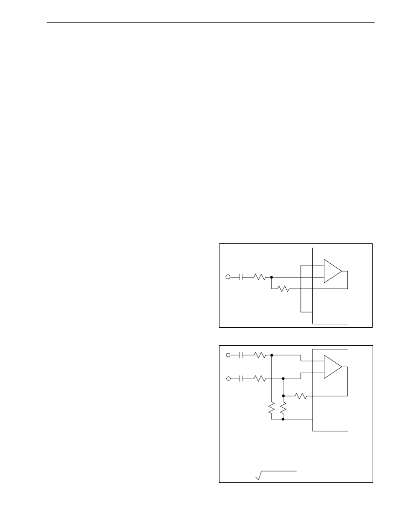
Figure 3 - Single Ended Input Configuration
Figure 4 - Differential Input Configuration
C
R
IN
IN+
IN-
GS
V
REF
Passband Voltage Gain
A
V
= R
F
/ R
IN
Highpass Corner Frequency
f
-3dB
= 1/(2
π
R
IN
C)
R
F
C1
R1
C2
R2
R4
R5
R3
IN+
IN-
GS
V
REF
Differential Input Amplifier
C1 = C2
R2 = R1 (For unity gain R3= R1)
R4 = (R3R5) / (R3 + R5)
Passband Voltage Gain
(A
V
diff) = R3/R1
Input Impedance
R
1
2
+ (1/
ω
C
1
)
2
(Z
IN
diff) = 2
Highpass Corner Frequency
f
-3dB
= 1/(2
π
R
1
C
1
)
相關(guān)PDF資料 |
PDF描述 |
|---|---|
| MT88EBNR | 4-Wire Calling Number Identification Circuit 2 (4-Wire CNIC2) |
| MT88L70AE1 | 3 Volt Integrated DTMF Receiver |
| MT88L70AE | 3 Volt Integrated DTMF Receiver |
| MT88L70AN | 3 Volt Integrated DTMF Receiver |
| MT88L70AN1 | 3 Volt Integrated DTMF Receiver |
相關(guān)代理商/技術(shù)參數(shù) |
參數(shù)描述 |
|---|---|
| MT88E46AS1 | 制造商:Microsemi Corporation 功能描述:CALLER ID CMOS 3.58MHZ 3.3V/5V 20SOIC - Rail/Tube |
| MT88E46ASR | 制造商:Microsemi Corporation 功能描述:CALLER ID CMOS 3.58MHZ 3.3V/5V 20SOIC - Tape and Reel |
| MT88E46ASR1 | 制造商:Microsemi Corporation 功能描述:CALLER ID CMOS 3.58MHZ 3.3V/5V 20SOIC - Tape and Reel |
| MT88EBNR | 制造商:ZARLINK 制造商全稱:Zarlink Semiconductor Inc 功能描述:4-Wire Calling Number Identification Circuit 2 (4-Wire CNIC2) |
| MT88L70 | 制造商:ZARLINK 制造商全稱:Zarlink Semiconductor Inc 功能描述:3 Volt Integrated DTMF Receiver |
發(fā)布緊急采購,3分鐘左右您將得到回復(fù)。