- 您現(xiàn)在的位置:買(mǎi)賣(mài)IC網(wǎng) > PDF目錄359232 > MT88E46AS (ZARLINK SEMICONDUCTOR INC) Bellcore Compliant Calling Number Identification Circuit PDF資料下載
參數(shù)資料
| 型號(hào): | MT88E46AS |
| 廠(chǎng)商: | ZARLINK SEMICONDUCTOR INC |
| 元件分類(lèi): | 無(wú)繩電話(huà)/電話(huà) |
| 英文描述: | Bellcore Compliant Calling Number Identification Circuit |
| 中文描述: | TELEPHONE CALLING NO IDENT CKT, PDSO20 |
| 封裝: | 0.300 INCH, MS-013AC, SOIC-20 |
| 文件頁(yè)數(shù): | 2/23頁(yè) |
| 文件大小: | 522K |
| 代理商: | MT88E46AS |
第1頁(yè)當(dāng)前第2頁(yè)第3頁(yè)第4頁(yè)第5頁(yè)第6頁(yè)第7頁(yè)第8頁(yè)第9頁(yè)第10頁(yè)第11頁(yè)第12頁(yè)第13頁(yè)第14頁(yè)第15頁(yè)第16頁(yè)第17頁(yè)第18頁(yè)第19頁(yè)第20頁(yè)第21頁(yè)第22頁(yè)第23頁(yè)
MT88E46
Advance Information
2
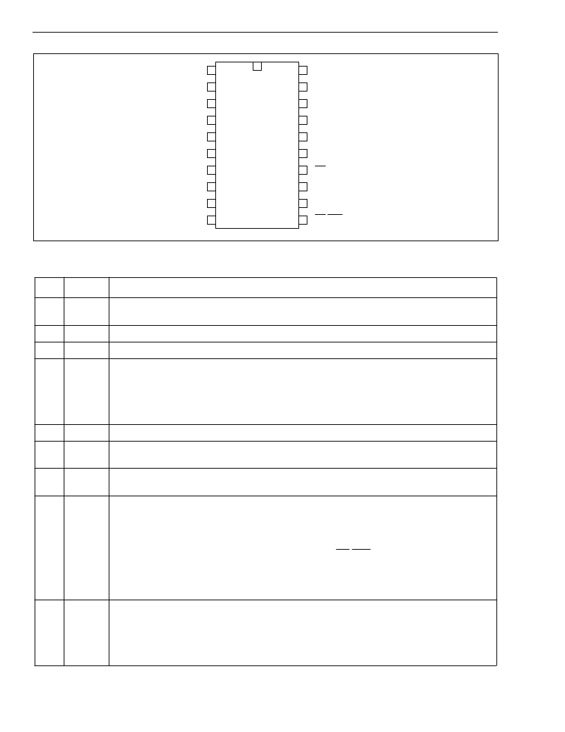
Figure 2 - Pin Connections
Pin Description
Pin #
Name
Description
1
V
REF
Voltage Reference (Output).
connection) and GS2 (telephone hybrid or speech IC receive pair connection) input op-amps.
Nominally Vdd/2. It is used to bias the GS1 (Tip/Ring
2
IN1+
GS1 Op-Amp Non-inverting Input.
The op-amp is for connecting the MT88E46 to Tip/Ring.
3
IN1-
GS1 Op-Amp Inverting Input.
The op-amp is for connecting the MT88E46 to Tip/Ring.
4
GS1
Gain Select 1 (Output).
connect the MT88E46 to Tip and Ring. The Tip/Ring signal can be amplified or attenuated at
GS1 via selection of the feedback resistor between GS1 and IN1-.
This is the output of the GS1 op-amp. The op-amp should be used to
FSK demodulation or ‘on hook mode’ CAS detection of the GS1 signal can be selected via the
CB1 and CB2 pins. See Tables 1 and 2.
5
Vss
Power Supply Ground.
6
OSC1
Oscillator Input.
clock source.
Crystal connection. This pin can also be driven directly from an external
7
OSC2
Oscillator Output.
should be left open circuit.
Crystal connection. When OSC1 is driven by an external clock, this pin
8
CB0
Control Bit 0 (CMOS Logic Input).
interface mode. When it is low, interface mode 0 is selected where the FSK bit stream is output
directly at the DATA pin. When it is high, interface mode 1 is selected where the FSK byte is
stored in a 1 byte buffer which can be read serially by the application’s microcontroller.
This pin is used primarily to select the 3-wire FSK data
The FSK interface is consisted of the DATA, DCLK and DR/DET pins. See the 3 pin
descriptions to understand how CB0 affects the FSK interface.
This pin is also used with CB1 and CB2 to put the MT88E46 into a power down state drawing
virtually no power supply current. See Tables 1 and 2.
9
DCLK
3-Wire FSK Interface Data Clock (Schmitt Logic Input/CMOS Logic Output).
mode 0 (when the CB0 pin is logic low) this is a CMOS output whose rising edge denotes the
nominal mid-point of a bit in the FSK data byte.
In interface
In interface mode 1 (when the CB0 pin is logic high) this is a Schmitt trigger input used to shift
the FSK data byte out of an on chip buffer to the DATA pin.
1
2
3
4
5
6
9
10
20
19
18
17
16
15
14
13
V
REF
IN1+
IN1-
GS1
Vss
OSC1
DCLK
DATA
IN2+
IN2-
GS2
CB2
CB1
Vdd
CD
NC
MT88E46
7
OSC2
8
CB0
12
11
IC
DR/DET
相關(guān)PDF資料 |
PDF描述 |
|---|---|
| MT88EBNR | 4-Wire Calling Number Identification Circuit 2 (4-Wire CNIC2) |
| MT88L70AE1 | 3 Volt Integrated DTMF Receiver |
| MT88L70AE | 3 Volt Integrated DTMF Receiver |
| MT88L70AN | 3 Volt Integrated DTMF Receiver |
| MT88L70AN1 | 3 Volt Integrated DTMF Receiver |
相關(guān)代理商/技術(shù)參數(shù) |
參數(shù)描述 |
|---|---|
| MT88E46AS1 | 制造商:Microsemi Corporation 功能描述:CALLER ID CMOS 3.58MHZ 3.3V/5V 20SOIC - Rail/Tube |
| MT88E46ASR | 制造商:Microsemi Corporation 功能描述:CALLER ID CMOS 3.58MHZ 3.3V/5V 20SOIC - Tape and Reel |
| MT88E46ASR1 | 制造商:Microsemi Corporation 功能描述:CALLER ID CMOS 3.58MHZ 3.3V/5V 20SOIC - Tape and Reel |
| MT88EBNR | 制造商:ZARLINK 制造商全稱(chēng):Zarlink Semiconductor Inc 功能描述:4-Wire Calling Number Identification Circuit 2 (4-Wire CNIC2) |
| MT88L70 | 制造商:ZARLINK 制造商全稱(chēng):Zarlink Semiconductor Inc 功能描述:3 Volt Integrated DTMF Receiver |
發(fā)布緊急采購(gòu),3分鐘左右您將得到回復(fù)。