- 您現(xiàn)在的位置:買賣IC網 > PDF目錄359232 > MT88E41AN (ZARLINK SEMICONDUCTOR INC) CMOS Extended Voltage Calling Number Identification Circuit (ECNIC) PDF資料下載
參數(shù)資料
| 型號: | MT88E41AN |
| 廠商: | ZARLINK SEMICONDUCTOR INC |
| 元件分類: | 無繩電話/電話 |
| 英文描述: | CMOS Extended Voltage Calling Number Identification Circuit (ECNIC) |
| 中文描述: | TELEPHONE CALLING NO IDENT CKT, PDSO20 |
| 封裝: | SSOP-20 |
| 文件頁數(shù): | 3/16頁 |
| 文件大小: | 888K |
| 代理商: | MT88E41AN |
MT88E41
Data Sheet
SEMICMF.019
2
Office. The received data can be processed externally by a microcontroller, stored in memory, or displayed as
is, depending on the application.
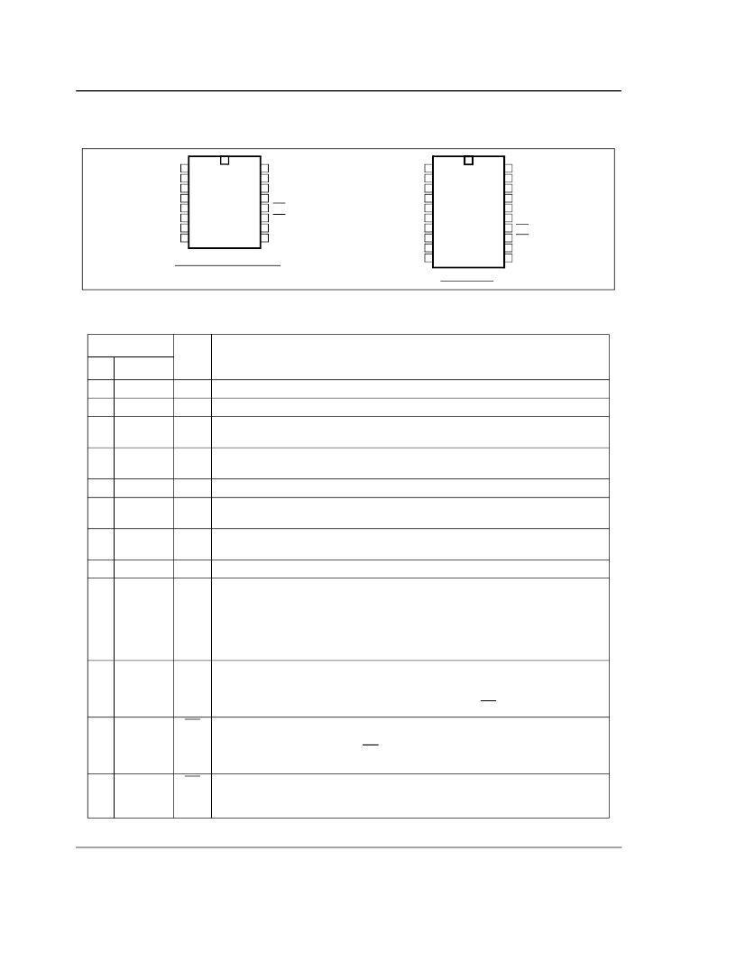
Figure 2 - Pin Connections
Pin Description Table
Pin
#
Name
Description
16
20
1
1
IN+
Non-inverting Op-Amp (Input).
2
2
IN-
Inverting Op-Amp (Input).
3
3
GS
Gain Select (Output).
Gives access to op-amp output for connection of feedback
resistor.
4
4
V
Ref
Voltage Reference (Output).
Nominally V
DD/2
. This is used to bias the op-amp
inputs.
Capacitor.
Connect a 0.1
μ
F capacitor to V
SS
.
OSC1
Oscillator (Input).
Crystal connection. This pin can be driven directly from an
external clocking source.
5
5
CAP
6
7
7
9
OSC2
Oscillator (Output).
Crystal connection. When OSC1 is driven by an external
clock, this pin should be left open.
8
10
V
SS
DCLK
Data Clock (Output).
Outputs a clock burst of 8 low going pulses at 1202.8Hz
(3.5795MHz divided by 2976). Every clock burst is initiated by the DATA stop bit
start bit sequence. When the input DATA is 1202.8 baud, the positive edge of each
DCLK pulse coincides with the middle of the data bits output at the DATA pin. No
DCLK pulses are generated during the start or stop bits. Typically, DCLK is used to
clock the eight data bits from the 10 bit data word into a serial-to-parallel converter.
Power supply ground.
9
11
10
12
DATA
Data (Output).
Serial data output corresponding to the FSK input and switching at
the input baud rate. Mark frequency at the input corresponds to a logic high, while
space frequency corresponds to a logic low at the DATA output. With no FSK
input, DATA is at logic high. This output stays high until CD
has become active.
11
13
DR
Data Ready (Open Drain Output).
This output goes low after the last DCLK pulse
of each word. This can be used to identify the data (8-bit word) boundary on the
serial output stream. Typically, DR is used to latch the eight data bits from the
serial-to-parallel converter into a microcontroller.
12
14
CD
Carrier Detect (Open Drain Output).
A logic low indicates that a carrier has been
present for a specified time on the line. A time hysteresis is provided to allow for
momentary discontinuity of carrier.
1
2
3
4
5
6
7
8
16
15
14
13
12
11
10
9
IN+
IN-
GS
VRef
CAP
OSC1
OSC2
VSS
VDD
IC2
IC1
PWDN
CD
DR
DATA
DCLK
16 PIN PLASTIC DIP/SOIC
1
2
3
4
5
6
7
8
9
10
11
12
20
19
18
17
16
15
14
13
IN+
IN-
GS
VRef
CAP
NC
OSC1
NC
OSC2
VSS
20 PIN SSOP
VDD
IC2
NC
NC
IC1
PWDN
CD
DR
DATA
DCLK
相關PDF資料 |
PDF描述 |
|---|---|
| MT88E41AS | CMOS Extended Voltage Calling Number Identification Circuit (ECNIC) |
| MT88E43 | Extended Voltage Calling Number Identification Circuit 2 |
| MT88E43AE | Extended Voltage Calling Number Identification Circuit 2 |
| MT88E43AS | Extended Voltage Calling Number Identification Circuit 2 |
| MT88E45B | 4-Wire Calling Number Identification Circuit 2 |
相關代理商/技術參數(shù) |
參數(shù)描述 |
|---|---|
| MT88E41AS | 制造商:ZARLINK 制造商全稱:Zarlink Semiconductor Inc 功能描述:CMOS Extended Voltage Calling Number Identification Circuit (ECNIC) |
| MT88E43 | 制造商:ZARLINK 制造商全稱:Zarlink Semiconductor Inc 功能描述:Extended Voltage Calling Number Identification Circuit 2 |
| MT88E43AE | 制造商:ZARLINK 制造商全稱:Zarlink Semiconductor Inc 功能描述:Extended Voltage Calling Number Identification Circuit 2 |
| MT88E43AS | 制造商:ZARLINK 制造商全稱:Zarlink Semiconductor Inc 功能描述:Extended Voltage Calling Number Identification Circuit 2 |
| MT88E43B | 制造商:ZARLINK 制造商全稱:Zarlink Semiconductor Inc 功能描述:Extended Voltage Calling Number Identification Circuit 2 |
發(fā)布緊急采購,3分鐘左右您將得到回復。