- 您現(xiàn)在的位置:買(mǎi)賣(mài)IC網(wǎng) > PDF目錄359218 > MRF6S20010GNR1 (飛思卡爾半導(dǎo)體(中國(guó))有限公司) RF Power Field Effect Transistors PDF資料下載
參數(shù)資料
| 型號(hào): | MRF6S20010GNR1 |
| 廠商: | 飛思卡爾半導(dǎo)體(中國(guó))有限公司 |
| 英文描述: | RF Power Field Effect Transistors |
| 中文描述: | 射頻功率場(chǎng)效應(yīng)晶體管 |
| 文件頁(yè)數(shù): | 1/24頁(yè) |
| 文件大小: | 591K |
| 代理商: | MRF6S20010GNR1 |
當(dāng)前第1頁(yè)第2頁(yè)第3頁(yè)第4頁(yè)第5頁(yè)第6頁(yè)第7頁(yè)第8頁(yè)第9頁(yè)第10頁(yè)第11頁(yè)第12頁(yè)第13頁(yè)第14頁(yè)第15頁(yè)第16頁(yè)第17頁(yè)第18頁(yè)第19頁(yè)第20頁(yè)第21頁(yè)第22頁(yè)第23頁(yè)第24頁(yè)
1
RF Device Data
Freescale Semiconductor
RF Power Field Effect Transistors
N-Channel Enhancement-Mode Lateral MOSFETs
Designed for Class A or Class AB general purpose applications with
frequencies from 1600 to 2200 MHz. Suitable for analog and digital modulation
and multipurpose amplifier applications.
Typical Two-Tone Performance @ 2170 MHz: V
DD
= 28 Volts, I
DQ
=
130 mA, P
out
= 10 Watts PEP
Power Gain — 15.5 dB
Drain Efficiency — 36%
IMD — -34 dBc
Typical 2-Carrier W-CDMA Performance: V
DD
= 28 Volts, I
DQ
= 130 mA,
P
out
= 1 Watt Avg., Full Frequency Band (2130-2170 MHz), Channel
Bandwidth = 3.84 MHz. PAR = 8.5 dB @ 0.01% Probability
Power Gain — 15.5 dB
Drain Efficiency — 15%
IM3 @ 10 MHz Offset — -47 dBc in 3.84 MHz Channel Bandwidth
ACPR @ 5 MHz Offset — -49 dBc in 3.84 MHz Channel Bandwidth
Typical Single-Carrier N-CDMA Performance: V
DD
= 28 Volts, I
DQ
=
130 mA, P
out
= 1 Watt Avg., Full Frequency Band (1930-1990 MHz),
IS-95 (Pilot, Sync, Paging, Traffic Codes 8 through 13), Channel Band-
width = 1.2288 MHz. PAR = 9.8 dB @ 0.01% Probability on CCDF.
Power Gain — 15.5 dB
Drain Efficiency— 16%
ACPR @ 885 kHz Offset = -60 dBc in 30 kHz Bandwidth
Typical GSM EDGE Performance: V
DD
= 28 Volts, I
DQ
= 130 mA, P
out
=
4 Watts Avg., Full Frequency Band (1805-1880 MHz)
Power Gain — 16 dB
Drain Efficiency — 33%
EVM — 1.3% rms
Capable of Handling 5:1 VSWR, @ 28 Vdc, 2000 MHz, 10 Watts CW
Output Power
Features
Characterized with Series Equivalent Large-Signal Impedance Parameters
Internally Matched for Ease of Use
Qualified Up to a Maximum of 32 V
DD
Operation
Integrated ESD Protection
200
°
C Capable Plastic Package
RoHS Compliant
In Tape and Reel. R1 Suffix = 500 Units per 24 mm, 13 inch Reel.
Table 1. Maximum Ratings
Rating
Symbol
Value
Unit
Drain-Source Voltage
V
DSS
-0.5, +68
Vdc
Gate-Source Voltage
V
GS
-0.5, +12
Vdc
Storage Temperature Range
T
stg
-65 to +175
°
C
Operating Junction Temperature
T
J
200
°
C
Document Number: MRF6S20010N
Rev. 1, 5/2006
Freescale Semiconductor
Technical Data
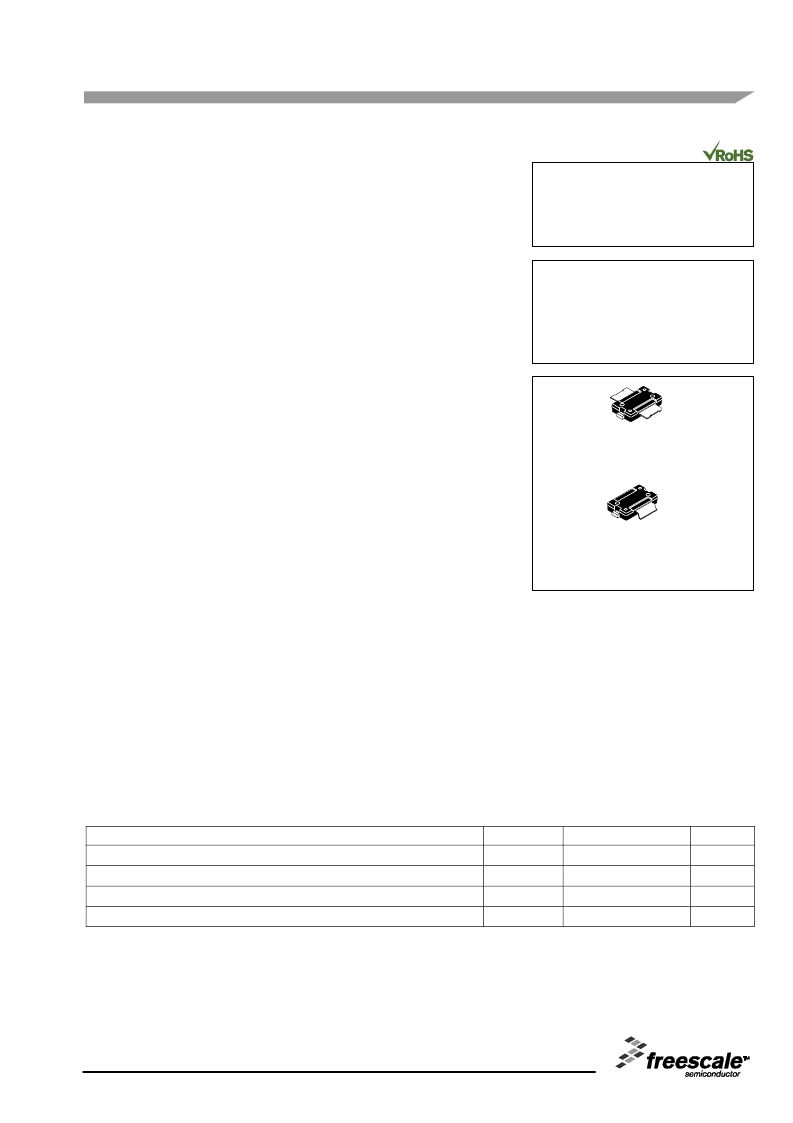
1600-2200 MHz, 10 W, 28 V
GSM/GSM EDGE
SINGLE N-CDMA
2 x W-CDMA
LATERAL N-CHANNEL
RF POWER MOSFETs
MRF6S20010NR1
MRF6S20010GNR1
CASE 1265-08, STYLE 1
TO-270-2
PLASTIC
MRF6S20010NR1
CASE 1265A-02, STYLE 1
TO-270-2 GULL
PLASTIC
MRF6S20010GNR1
Freescale Semiconductor, Inc., 2006. All rights reserved.
相關(guān)PDF資料 |
PDF描述 |
|---|---|
| MRF6S21050LR3 | RF Power Field Effect Transistors |
| MRF6S21050LSR3 | RF Power Field Effect Transistors |
| MRF6S21060NBR1 | RF Power Field Effect Transistors N-Channel Enhancement-Mode Lateral MOSFETs |
| MRF6S21100HR3 | RF Power Field Effect Transistors N-Channel Enhancement-Mode Lateral MOSFETs |
| MRF6S21100HSR3 | RF Power Field Effect Transistors N-Channel Enhancement-Mode Lateral MOSFETs |
相關(guān)代理商/技術(shù)參數(shù) |
參數(shù)描述 |
|---|---|
| MRF6S20010GNR1-CUT TAPE | 制造商:Freescale 功能描述:MRF6S20010 Series 1.6 to 2.2 GHz 28 V 10 W RF Power N-Ch Mosfet - TO-270 |
| MRF6S20010NR1 | 功能描述:射頻MOSFET電源晶體管 HV6 2GHZ 10W TO270-2 RoHS:否 制造商:Freescale Semiconductor 配置:Single 晶體管極性: 頻率:1800 MHz to 2000 MHz 增益:27 dB 輸出功率:100 W 汲極/源極擊穿電壓: 漏極連續(xù)電流: 閘/源擊穿電壓: 最大工作溫度: 封裝 / 箱體:NI-780-4 封裝:Tray |
| MRF6S20010NR1_09 | 制造商:FREESCALE 制造商全稱(chēng):Freescale Semiconductor, Inc 功能描述:RF Power Field Effect Transistors N-Channel Enhancement-Mode Lateral MOSFETs |
| MRF6S21050LR3 | 功能描述:射頻MOSFET電源晶體管 HV6 W-CDMA 11.5W NI400L RoHS:否 制造商:Freescale Semiconductor 配置:Single 晶體管極性: 頻率:1800 MHz to 2000 MHz 增益:27 dB 輸出功率:100 W 汲極/源極擊穿電壓: 漏極連續(xù)電流: 閘/源擊穿電壓: 最大工作溫度: 封裝 / 箱體:NI-780-4 封裝:Tray |
| MRF6S21050LR3_08 | 制造商:FREESCALE 制造商全稱(chēng):Freescale Semiconductor, Inc 功能描述:RF Power Field Effect Transistors N-Channel Enhancement-Mode Lateral MOSFETs |
發(fā)布緊急采購(gòu),3分鐘左右您將得到回復(fù)。