- 您現(xiàn)在的位置:買賣IC網(wǎng) > PDF目錄359188 > MPC5534 (飛思卡爾半導(dǎo)體(中國)有限公司) Microcontroller PDF資料下載
參數(shù)資料
| 型號: | MPC5534 |
| 廠商: | 飛思卡爾半導(dǎo)體(中國)有限公司 |
| 英文描述: | Microcontroller |
| 中文描述: | 微控制器 |
| 文件頁數(shù): | 4/50頁 |
| 文件大小: | 1148K |
| 代理商: | MPC5534 |
第1頁第2頁第3頁當(dāng)前第4頁第5頁第6頁第7頁第8頁第9頁第10頁第11頁第12頁第13頁第14頁第15頁第16頁第17頁第18頁第19頁第20頁第21頁第22頁第23頁第24頁第25頁第26頁第27頁第28頁第29頁第30頁第31頁第32頁第33頁第34頁第35頁第36頁第37頁第38頁第39頁第40頁第41頁第42頁第43頁第44頁第45頁第46頁第47頁第48頁第49頁第50頁
MPC5534 Microcontroller Data Sheet, Rev. 0
Preliminary—Subject to Change Without Notice
Electrical Characteristics
Freescale Semiconductor
4
3
Electrical Characteristics
This section contains detailed information on power considerations, DC/AC electrical characteristics, and
AC timing specifications for the MCU.
3.1
Maximum Ratings
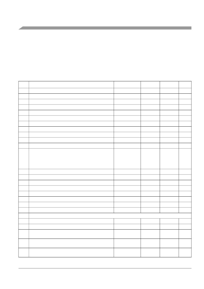
Table 2. Absolute Maximum Ratings
1
Num
Characteristic
Symbol
Min
Max
2
Unit
1
1.5V Core Supply Voltage
3
V
DD
V
PP
V
DDF
V
FLASH
V
STBY
V
DDSYN
V
DD33
V
RC33
V
DDA
V
DDE
V
DDEH
V
IN
– 0.3
1.7
V
2
Flash Program/Erase Voltage
– 0.3
6.5
V
3
Flash Core Voltage
– 0.3
1.7
V
4
Flash Read Voltage
– 0.3
4.6
V
5
SRAM Standby Voltage
– 0.3
1.7
V
6
Clock Synthesizer Voltage
– 0.3
4.6
V
7
3.3V I/O Buffer Voltage
–0.3
4.6
V
8
Voltage Regulator Control Input Voltage
–0.3
4.6
V
9
Analog Supply Voltage (reference to V
SSA
)
I/O Supply Voltage (Fast I/O Pads)
4
I/O Supply Voltage (Slow/Medium I/O Pads)
4
DC Input Voltage
5
VDDEH powered I/O Pads, except eTPUB15 and
SINB (DSPI_B_SIN)
VDDEH powered I/O Pads (eTPUB15 and SINB)
VDDE powered I/O Pads
– 0.3
5.5
V
10
– 0.3
4.6
V
11
– 0.3
6.5
V
12
–1.0
6
–0.3
7
–1.0
6
6.5
8
6.5
8
4.6
9
V
13
Analog Reference High Voltage (reference to VRL)
V
RH
– 0.3
5.5
V
14
VSS Differential Voltage
V
SS
– V
SSA
V
DD
– V
DDA
V
RH
– V
RL
V
RH
– V
DDA
V
RL
– V
SSA
V
DDEH
– V
DDA
V
DDF
– V
DD
– 0.1
0.1
V
15
VDD Differential Voltage
– V
DDA
– 0.3
V
DD
5.5
V
16
V
REF
Differential Voltage
V
RH
to VDDA Differential Voltage
V
RL
to VSSA Differential Voltage
V
DDEH
to V
DDA
Differential Voltage
V
DDF
to V
DD
Differential Voltage
This spec has been moved to
Table 9
, spec 43a.
V
17
– 5.5
5.5
V
18
– 0.3
0.3
V
19
–V
DDA
–0.3
V
DDEH
0.3
V
20
V
21
22
VSSSYN to VSS Differential Voltage
V
SSSYN
– V
SS
V
RCVSS
– V
SS
I
MAXD
–0.1
0.1
V
23
V
RCVSS
to V
SS
Differential Voltage
Maximum DC Digital Input Current
10
(per pin, applies to all
digital pins)
5
Maximum DC Analog Input Current
11
(per pin, applies to all
analog pins)
Maximum Operating Temperature Range
12
— Die Junction
Temperature
–0.1
0.1
V
24
–2
2
mA
25
I
MAXA
–3
3
mA
26
T
J
– 40.0
150.0
o
C
相關(guān)PDF資料 |
PDF描述 |
|---|---|
| MPC7447A | PowerPC microprocessor |
| MPC7447ANXPNS | PowerPC microprocessor |
| MPC7455 | RISC Microprocessor Hardware Specifications |
| MPC7457 | RISC Microprocessor Hardware Specifications |
| MPC7457EC | RISC Microprocessor Hardware Specifications |
相關(guān)代理商/技術(shù)參數(shù) |
參數(shù)描述 |
|---|---|
| MPC5534AVF40 | 制造商:FREESCALE 制造商全稱:Freescale Semiconductor, Inc 功能描述:Microcontroller |
| MPC5534AVF40R2 | 制造商:FREESCALE 制造商全稱:Freescale Semiconductor, Inc 功能描述:Microcontroller |
| MPC5534AVF66 | 制造商:FREESCALE 制造商全稱:Freescale Semiconductor, Inc 功能描述:Microcontroller |
| MPC5534AVF66R2 | 制造商:FREESCALE 制造商全稱:Freescale Semiconductor, Inc 功能描述:Microcontroller |
| MPC5534AVF80 | 制造商:FREESCALE 制造商全稱:Freescale Semiconductor, Inc 功能描述:Microcontroller |
發(fā)布緊急采購,3分鐘左右您將得到回復(fù)。