- 您現(xiàn)在的位置:買賣IC網(wǎng) > PDF目錄359188 > MPC5534 (飛思卡爾半導(dǎo)體(中國)有限公司) Microcontroller PDF資料下載
參數(shù)資料
| 型號: | MPC5534 |
| 廠商: | 飛思卡爾半導(dǎo)體(中國)有限公司 |
| 英文描述: | Microcontroller |
| 中文描述: | 微控制器 |
| 文件頁數(shù): | 15/50頁 |
| 文件大?。?/td> | 1148K |
| 代理商: | MPC5534 |
第1頁第2頁第3頁第4頁第5頁第6頁第7頁第8頁第9頁第10頁第11頁第12頁第13頁第14頁當(dāng)前第15頁第16頁第17頁第18頁第19頁第20頁第21頁第22頁第23頁第24頁第25頁第26頁第27頁第28頁第29頁第30頁第31頁第32頁第33頁第34頁第35頁第36頁第37頁第38頁第39頁第40頁第41頁第42頁第43頁第44頁第45頁第46頁第47頁第48頁第49頁第50頁
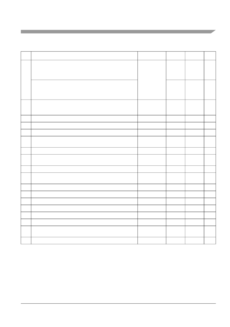
Electrical Characteristics
MPC5534 Microcontroller Data Sheet, Rev. 0
Preliminary—Subject to Change Without Notice
Freescale Semiconductor
15
31
Fast I/O Weak Pull Up Current
11
1.62V – 1.98V
2.25V – 2.75V
3.0V – 3.6V
I
ACT_F
10
20
20
110
130
170
μ
A
μ
A
μ
A
Fast I/O Weak Pull Down Current
11
1.62V – 1.98V
2.25V – 2.75V
3.0V – 3.6V
10
20
20
100
130
170
μ
A
μ
A
μ
A
32
Slow/Medium I/O Weak Pull Up/Down Current
12
3.0V – 3.6V
4.5V – 5.5V
I
ACT_S
10
20
150
170
μ
A
μ
A
33
I/O Input Leakage Current
13
I
INACT_D
– 2.5
2.5
μ
A
34
DC Injection Current (per pin)
I
IC
– 2.0
2.0
mA
35
Analog Input Current, Channel Off
14
I
INACT_A
–150
150
nA
35a Analog Input Current, Shared Analog/Digital pins
(AN12, AN13, AN14, AN15)
I
INACT_AD
– 2.5
2.5
μ
A
36
VSS Differential Voltage
15
VSS – VSSA
– 100
100
mV
37
Analog Reference Low Voltage
VRL
VSSA –
0.1
VSSA +
0.1
V
38
VRL Differential Voltage
VRL – VSSA
–100
100
mV
39
Analog Reference High Voltage
VRH
VDDA –
0.1
VDDA +
0.1
V
40
V
REF
Differential Voltage
VRH – VRL
4.5
5.25
V
41
VSSSYN to VSS Differential Voltage
VSSSYN – VSS
–50
50
mV
42
VRCVSS to VSS Differential Voltage
VRCVSS – VSS
–50
50
mV
43
VDDF to VDD Differential Voltage
2
VDDF – VDD
–100
100
mV
43a VRC33 to VDDSYN Differential Voltage
V
RC33
– V
DDSYN
–0.1
0.1
16
V
44
Analog Input Differential Signal Range (with common mode 2.5V)
V
IDIFF
– 2.5
2.5
V
45
Operating Temperature Range — Ambient (Packaged)
T
A
(T
L
to T
H
)
– 40.0
125.0
ο
C
46
Slew rate on power supply pins
—
—
50
V/ms
1
| VDDA0–VDDA1 | must be < 0.1V
2
VPP can drop to 3.0 volts during read operations.
3
During standby operation. If standby operation is not required, VSTBY can be connected to ground.
4
Applies to CLKOUT, external bus pins, and Nexus pins.
5
Maximum average RMS DC current.
6
Peak currents may be higher on specialized code.
Table 9. DC Electrical Specifications (continued)
Num
Characteristic
Symbol
Min
Max
Unit
相關(guān)PDF資料 |
PDF描述 |
|---|---|
| MPC7447A | PowerPC microprocessor |
| MPC7447ANXPNS | PowerPC microprocessor |
| MPC7455 | RISC Microprocessor Hardware Specifications |
| MPC7457 | RISC Microprocessor Hardware Specifications |
| MPC7457EC | RISC Microprocessor Hardware Specifications |
相關(guān)代理商/技術(shù)參數(shù) |
參數(shù)描述 |
|---|---|
| MPC5534AVF40 | 制造商:FREESCALE 制造商全稱:Freescale Semiconductor, Inc 功能描述:Microcontroller |
| MPC5534AVF40R2 | 制造商:FREESCALE 制造商全稱:Freescale Semiconductor, Inc 功能描述:Microcontroller |
| MPC5534AVF66 | 制造商:FREESCALE 制造商全稱:Freescale Semiconductor, Inc 功能描述:Microcontroller |
| MPC5534AVF66R2 | 制造商:FREESCALE 制造商全稱:Freescale Semiconductor, Inc 功能描述:Microcontroller |
| MPC5534AVF80 | 制造商:FREESCALE 制造商全稱:Freescale Semiconductor, Inc 功能描述:Microcontroller |
發(fā)布緊急采購,3分鐘左右您將得到回復(fù)。