- 您現(xiàn)在的位置:買賣IC網(wǎng) > PDF目錄359188 > MPC5200 (飛思卡爾半導(dǎo)體(中國)有限公司) Hardware Specifications PDF資料下載
參數(shù)資料
| 型號: | MPC5200 |
| 廠商: | 飛思卡爾半導(dǎo)體(中國)有限公司 |
| 英文描述: | Hardware Specifications |
| 中文描述: | 硬件規(guī)格 |
| 文件頁數(shù): | 19/80頁 |
| 文件大小: | 790K |
| 代理商: | MPC5200 |
第1頁第2頁第3頁第4頁第5頁第6頁第7頁第8頁第9頁第10頁第11頁第12頁第13頁第14頁第15頁第16頁第17頁第18頁當(dāng)前第19頁第20頁第21頁第22頁第23頁第24頁第25頁第26頁第27頁第28頁第29頁第30頁第31頁第32頁第33頁第34頁第35頁第36頁第37頁第38頁第39頁第40頁第41頁第42頁第43頁第44頁第45頁第46頁第47頁第48頁第49頁第50頁第51頁第52頁第53頁第54頁第55頁第56頁第57頁第58頁第59頁第60頁第61頁第62頁第63頁第64頁第65頁第66頁第67頁第68頁第69頁第70頁第71頁第72頁第73頁第74頁第75頁第76頁第77頁第78頁第79頁第80頁
Electrical and Thermal Characteristics
MPC5200 Data Sheet, Rev. 4
Freescale Semiconductor
19
Notes:
1) The frequency of IP_CLK depends on register settings in Clock Distribution Module. See the MPC5200 User Manual [1].
2) The interrupt latency descriptions in the table above are related to non competitive, non masked but enabled external
interrupt sources. Take care of interrupt prioritization which may increase the latencies.
Since all external interrupt signals are synchronized into the internal processor bus clock domain, each of
these signals has to exceed a minimum pulse width of more than one IP_CLK cycle.
NOTES:
1) The frequency of the IP_CLK depends on the register settings in Clock Distribution Module. See the MPC5200 User Manual
[1] for further information.
2) If the same interrupt occurs a second time while its interrupt service routine has not cleared the former one, the second
interrupt will not be recognized at all.
Besides synchronization, prioritization, and mapping the latency of an external interrupt to the start of its
associated interrupt service routine also depends on the following conditions: To get a minimum interrupt
service response time, it is recommended to enable the instruction cache and set up the maximum core
clock, XL bus, and IP bus frequencies (depending on board design and programming). In addition, it is
advisable to execute an interrupt handler, which has been implemented in assembly code.
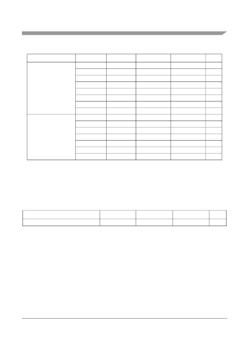
Standard GPIO Interrupts
GPIO_PSC3_4
12
IP_CLK
normal (int)
A4.7
GPIO_PSC3_5
GPIO_PSC3_8
12
IP_CLK
normal (int)
A4.8
12
IP_CLK
normal (int)
A4.9
GPIO_USB_9
12
IP_CLK
normal (int)
A4.10
GPIO_ETHI_4
12
IP_CLK
normal (int)
A4.11
GPIO_ETHI_5
12
IP_CLK
normal (int)
A4.12
GPIO_ETHI_6
12
IP_CLK
normal (int)
A4.13
GPIO_
ETHI_7
GPIO_
PSC1_4
GPIO_PSC2_4
12
IP_CLK
normal (int)
A4.14
GPIO WakeUp Interrupts
12
IP_CLK
normal (int)
A4.15
12
IP_CLK
normal (int)
A4.16
GPIO_PSC3_9
12
IP_CLK
normal (int)
A4.17
GPIO_ETHI_8
12
IP_CLK
normal (int)
A4.18
GPIO_IRDA_0
12
IP_CLK
normal (int)
A4.19
DGP_IN0
12
IP_CLK
normal (int)
A4.20
DGP_IN1
12
IP_CLK
normal (int)
A4.21
Table 17. Minimum pulse width for external interrupts to be recognized
Name
Min Pulse Width
Max Pulse Width
Reference Clock
SpecID
All external interrupts (IRQs, GPIOs)
> 1 clock cycle
—
IP_CLK
A4.22
Table 16. External interrupt latencies (continued)
Interrupt Type
Pin Name
Clock Cycles
Reference Clock
Core Interrupt
SpecID
相關(guān)PDF資料 |
PDF描述 |
|---|---|
| MPC5534 | Microcontroller |
| MPC7447A | PowerPC microprocessor |
| MPC7447ANXPNS | PowerPC microprocessor |
| MPC7455 | RISC Microprocessor Hardware Specifications |
| MPC7457 | RISC Microprocessor Hardware Specifications |
相關(guān)代理商/技術(shù)參數(shù) |
參數(shù)描述 |
|---|---|
| MPC5200B | 制造商:FREESCALE 制造商全稱:Freescale Semiconductor, Inc 功能描述:SDRAM/DDR Memory Controller |
| MPC5200B_08 | 制造商:FREESCALE 制造商全稱:Freescale Semiconductor, Inc 功能描述:SDRAM / DDR Memory Controller |
| MPC5200B_10 | 制造商:FREESCALE 制造商全稱:Freescale Semiconductor, Inc 功能描述:SDRAM/DDR Memory Controller |
| MPC5200BDS | 制造商:FREESCALE 制造商全稱:Freescale Semiconductor, Inc 功能描述:Technical Data |
| MPC5200BV400 | 功能描述:微處理器 - MPU 400MHz 760MIPS RoHS:否 制造商:Atmel 處理器系列:SAMA5D31 核心:ARM Cortex A5 數(shù)據(jù)總線寬度:32 bit 最大時(shí)鐘頻率:536 MHz 程序存儲器大小:32 KB 數(shù)據(jù) RAM 大小:128 KB 接口類型:CAN, Ethernet, LIN, SPI,TWI, UART, USB 工作電源電壓:1.8 V to 3.3 V 最大工作溫度:+ 85 C 安裝風(fēng)格:SMD/SMT 封裝 / 箱體:FBGA-324 |
發(fā)布緊急采購,3分鐘左右您將得到回復(fù)。