- 您現(xiàn)在的位置:買賣IC網(wǎng) > PDF目錄359150 > MC9S12H128 (Motorola, Inc.) Device User Guide PDF資料下載
參數(shù)資料
| 型號: | MC9S12H128 |
| 廠商: | Motorola, Inc. |
| 英文描述: | Device User Guide |
| 中文描述: | 設(shè)備用戶指南 |
| 文件頁數(shù): | 64/124頁 |
| 文件大小: | 2125K |
| 代理商: | MC9S12H128 |
第1頁第2頁第3頁第4頁第5頁第6頁第7頁第8頁第9頁第10頁第11頁第12頁第13頁第14頁第15頁第16頁第17頁第18頁第19頁第20頁第21頁第22頁第23頁第24頁第25頁第26頁第27頁第28頁第29頁第30頁第31頁第32頁第33頁第34頁第35頁第36頁第37頁第38頁第39頁第40頁第41頁第42頁第43頁第44頁第45頁第46頁第47頁第48頁第49頁第50頁第51頁第52頁第53頁第54頁第55頁第56頁第57頁第58頁第59頁第60頁第61頁第62頁第63頁當(dāng)前第64頁第65頁第66頁第67頁第68頁第69頁第70頁第71頁第72頁第73頁第74頁第75頁第76頁第77頁第78頁第79頁第80頁第81頁第82頁第83頁第84頁第85頁第86頁第87頁第88頁第89頁第90頁第91頁第92頁第93頁第94頁第95頁第96頁第97頁第98頁第99頁第100頁第101頁第102頁第103頁第104頁第105頁第106頁第107頁第108頁第109頁第110頁第111頁第112頁第113頁第114頁第115頁第116頁第117頁第118頁第119頁第120頁第121頁第122頁第123頁第124頁
MC9S12DP512 Device Guide V01.23
64
2.3.55 PS2 / RXD1 — Port S I/O Pin 2
PS2 is a general purpose input or output pin. It can be configured as the receive pin RXD of Serial
Communication Interface 1 (SCI1).
2.3.56 PS1 / TXD0 — Port S I/O Pin 1
PS1 is a general purpose input or output pin. It can be configured as the transmit pin TXD of Serial
Communication Interface 0 (SCI0).
2.3.57 PS0 / RXD0 — Port S I/O Pin 0
PS0 is a general purpose input or output pin. It can be configured as the receive pin RXD of Serial
Communication Interface 0 (SCI0).
2.3.58 PT[7:0] / IOC[7:0] — Port T I/O Pins [7:0]
PT7-PT0 are general purpose input or output pins. They can be configured as input capture or output
compare pins IOC7-IOC0 of the Enhanced Capture Timer (ECT).
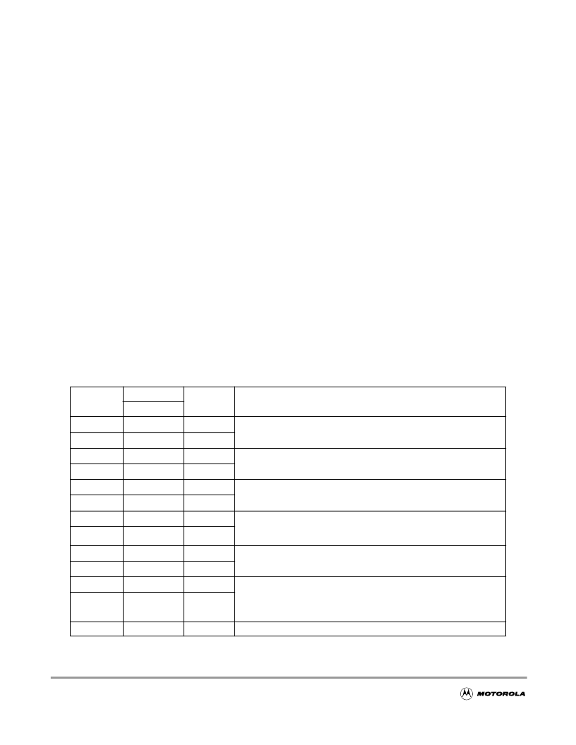
2.4 Power Supply Pins
MC9S12DP512 power and ground pins are described below.
Table 2-2 MC9S12DP512 Power and Ground Connection Summary
Pin Number
Nominal
Voltage
112-pin QFP
V
DD1, 2
13, 65
2.5 V
Internal power and ground generated by internal regulator
V
SS1, 2
14, 66
0V
V
DDR
41
5.0 V
External power and ground, supply to pin drivers and internal voltage
regulator.
V
SSR
40
0 V
V
DDX
107
5.0 V
External power and ground, supply to pin drivers.
V
SSX
106
0 V
V
DDA
83
5.0 V
Operating voltage and ground for the analog-to-digital converters and
the reference for the internal voltage regulator, allows the supply
voltage to the A/D to be bypassed independently.
86
0 V
V
RL
85
0 V
Reference voltages for the analog-to-digital converter.
V
RH
84
5.0 V
V
DDPLL
43
2.5 V
Provides operating voltage and ground for the Phased-Locked Loop.
This allows the supply voltage to the PLL to be bypassed
independently. Internal power and ground generated by internal
regulator.
VREGEN
97
5V
Internal Voltage Regulator enable/disable
Mnemonic
Description
V
SSA
V
SSPLL
45
0 V
F
For More Information On This Product,
Go to: www.freescale.com
n
.
相關(guān)PDF資料 |
PDF描述 |
|---|---|
| MC9S12A256 | MC9S12DT256 Device User Guide V03.03 |
| MC9S12A128 | MC9S12DT128 Device User Guide V02.09 |
| MC9S12A12 | MC9S12DT128 Device User Guide V02.09 |
| MC9S12DB128 | MC9S12DT128 Device User Guide V02.09 |
| MC9S12DJ128E | MC9S12DT128 Device User Guide V02.09 |
相關(guān)代理商/技術(shù)參數(shù) |
參數(shù)描述 |
|---|---|
| MC9S12H128VFVE | 功能描述:16位微控制器 - MCU 16B FLASH CANS 2XAT RoHS:否 制造商:Texas Instruments 核心:RISC 處理器系列:MSP430FR572x 數(shù)據(jù)總線寬度:16 bit 最大時鐘頻率:24 MHz 程序存儲器大小:8 KB 數(shù)據(jù) RAM 大小:1 KB 片上 ADC:Yes 工作電源電壓:2 V to 3.6 V 工作溫度范圍:- 40 C to + 85 C 封裝 / 箱體:VQFN-40 安裝風(fēng)格:SMD/SMT |
| MC9S12H128VPV | 制造商:Rochester Electronics LLC 功能描述:- Bulk |
| MC9S12H128VPVE | 功能描述:16位微控制器 - MCU 16B FLASH CANS 2XAT RoHS:否 制造商:Texas Instruments 核心:RISC 處理器系列:MSP430FR572x 數(shù)據(jù)總線寬度:16 bit 最大時鐘頻率:24 MHz 程序存儲器大小:8 KB 數(shù)據(jù) RAM 大小:1 KB 片上 ADC:Yes 工作電源電壓:2 V to 3.6 V 工作溫度范圍:- 40 C to + 85 C 封裝 / 箱體:VQFN-40 安裝風(fēng)格:SMD/SMT |
| MC9S12H256VFV | 功能描述:16位微控制器 - MCU 16 Bit 16MHz RoHS:否 制造商:Texas Instruments 核心:RISC 處理器系列:MSP430FR572x 數(shù)據(jù)總線寬度:16 bit 最大時鐘頻率:24 MHz 程序存儲器大小:8 KB 數(shù)據(jù) RAM 大小:1 KB 片上 ADC:Yes 工作電源電壓:2 V to 3.6 V 工作溫度范圍:- 40 C to + 85 C 封裝 / 箱體:VQFN-40 安裝風(fēng)格:SMD/SMT |
| MC9S12H256VFVE | 功能描述:16位微控制器 - MCU 16B FLASH CANS 2XAT RoHS:否 制造商:Texas Instruments 核心:RISC 處理器系列:MSP430FR572x 數(shù)據(jù)總線寬度:16 bit 最大時鐘頻率:24 MHz 程序存儲器大小:8 KB 數(shù)據(jù) RAM 大小:1 KB 片上 ADC:Yes 工作電源電壓:2 V to 3.6 V 工作溫度范圍:- 40 C to + 85 C 封裝 / 箱體:VQFN-40 安裝風(fēng)格:SMD/SMT |
發(fā)布緊急采購,3分鐘左右您將得到回復(fù)。